As shown in Figure 1, VMMK devices reduce losses and parasitic circuit parameters from common RF surface mount packages due to Avago's unique wafer cavity process. By eliminating parasitic inductance and capacitance between the solder and package leads, a low loss and low impedance signal path is formed between the chip and the package. The cavity above the component has a low dielectric constant and is therefore capable of operating at high frequencies, and in addition the cavity provides mechanical protection in device applications.
Figure 1 Anwar high-cost semiconductor process
As shown in Figure 2, the input and output of the device are connected through the holes on the back of the wafer, eliminating the performance degradation caused by wire bonding. Avago’s VMMK metallization and sealing process ensures that the device can operate under standard soldering procedures.
The VMMK device process eliminates wire bonding and improves thermal characteristics to increase the stability of the patch. The VMMK device process does not add any new equipment to the surface-mount process, and the existing standard placement equipment fully meets the requirements.
Finally, by eliminating package pinouts, VMMK devices are thinner, lighter, and have a smaller layout area than conventional RF surface mount devices. For example, the VMMK-2x03 RF amplifier (1mm*0.5mm*0.25mm) requires only 5% of the volume and 10% of the PCB area of ​​the SOT-342 package. Compared to many standard RF surface mount packages, VMMK devices save at least 50% of the PCB area.
As parasitic effects are reduced, VMMK devices are directly connected to the PCB traces to reduce losses on the signal path. The cavity structure of the VMMK device can effectively reduce parasitic parameters and improve performance.
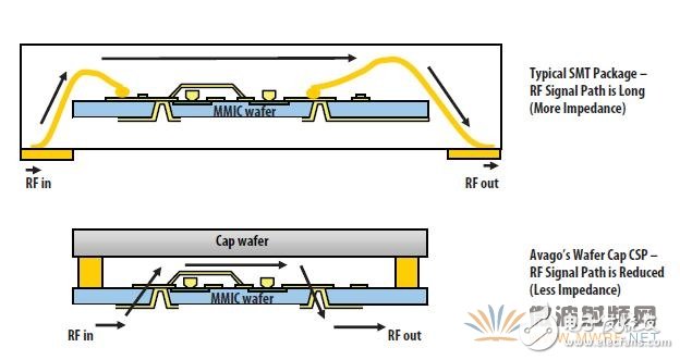
Figure 2 Avago wafer cavity process reduces RF loss and parasitic inductance
Excellent performance at low costThe Avago VMMK device process has a large range of semiconductor manufacturing capabilities. As shown in Figure 3, Avago VMMK device technology can achieve better performance at low cost by eliminating costly process steps in traditional SMT packages, such as gold wire, cell connections and SMT molding. The VMMK device is very small in size, as shown in Figure 4, and can accommodate up to 20 VMMK devices in the SOT-343 package.
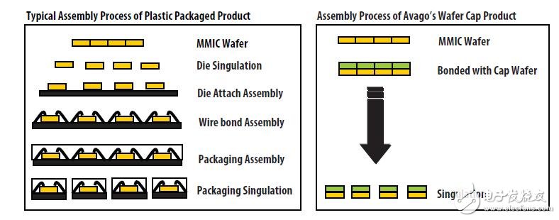
Figure 3 Low-cost VMMK devices for batch RF applications
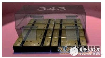
Figure 4 SOT-343 package can accommodate 20 VMMK devices
Simple assembly and product manufacturingVMMK devices do not require special PCB design, fabrication, and assembly processes for the user. Avago’s VMMK components can be adapted to any design that uses the SMT process and require only simple design and layout.
Standard PCB materialVMMK devices are limited to FR4 materials, and RO4003, RO4350 and 5880 plates are recommended for low insertion loss microwave materials. Welding of VMMK devices on PCBs requires greater thermal expansion than FR5, and the conversion temperature of FR4 cannot be used.
PCB layout considerationsThe package of the VMMK device is similar to the standard 0402 package capacitor. However, PCB engineers cannot use the standard 0402 package as a package for VMMK devices. The metallization in the VMMK device is soldered. The appropriate VMMK device package pads recommended by the chip data are shown in Figure 5 below. The solder mask should suppress solder flow around the pads. The gap between the pads cannot be bridged by solder flow. The material of the pad is a mixture of 5 micron gold and 1 micron nickel. When solder flows on the pad, the gold layer in the pad of the VMMK device dissolves, and the nickel layer and the solder melt and mix, which occurs mainly during the soldering of the device to the PCB.
The following is the VMMK device patch production guide1. There must be no through holes covering the solder mask on the PCB pads.
2. The welded steel mesh should ensure the amount of solder paste deposited on the pads. The shape of the stencil of the VMMK device is shown in Figure 6 below. For other welding information, refer to the ANWARA application document AN-5378.
3. VMMK devices require a standard deionized water cleaning process during the soldering process, eliminating the need for ultrasonic cleaning and gas phase cleaning.
4. The VMMK device uses a polymer material as the gasket material. This polymer material has been used for wafer passivation and chip package surfaces. Polymer materials are widely used in the PCB manufacturing and processing industries by Dow Chemical. VMMK devices use this material to achieve the best fit with PCB soldering. Other information on materials needs to be referenced in the application note AN-5378.
5. VMMK device in PCB design needs reference application document AN-5378
6. Solder paste for welding VMMK devices is recommended to be clean or water soluble.
7. The Avago VMMK device is tested for humidity sensitivity in accordance with MSL2a.
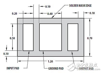
Figure 5 VMMK device land pattern
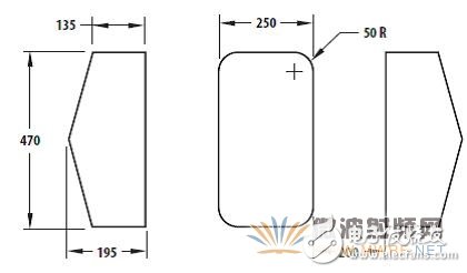
Figure 6 VMMK device welded steel mesh pattern
Chip packaging and mass production considerationsAvago VMMK devices are prohibited from over-packaging, which can cause damage to the cavity inside the device, which in turn affects the electrical performance of the device. VMMK devices can be mass-produced using standard PCB mount machining equipment, and both the Japanese heavy machine KE-2050RL and the Panasonic MSF NM-MD15 can be used.
Reflow Process GuideThe infrared temperature rise curve of the VMMK device is based on the J-STD-020 C version of the JEDEC/IPC standard. VMMK devices can withstand up to three reflow cycles under the J-STD-020 standard, and more than three reflow cycles reduce the contact surface between the metal portion of the wafer and the solder. Wave soldering or vapor phase reflow soldering cannot be used for VMMK devices. VMMK recommends reflow soldering as a through-flow furnace capable of transferring heat. Reflow soldering of VMMK devices is not difficult as long as the J-STD-020 standard and process guidelines are met. The recommended reflow soldering process guidelines are as follows:
1. Avoid preheating for too long to produce oxidation. Strict control of the temperature can not exceed 217 degrees, so as not to affect the integrity of the solder joint. Excessive reflow time can result in excessive metal compounds, solder surface passivation, and flux residue. Reflow soldering time of less than 30 seconds can result in solder and device soldering.
2. VMMK devices should be reflowed at the temperature and time of the lead-free soldering process. The time and rate of temperature rise and fall in reflow soldering refer to the J-STD-020C standard, otherwise it will cause board deformation and device damage caused by thermal stress. The reflow temperature should not exceed the peak temperature specified by the JEDED standard, otherwise it will cause internal damage to the VMMK device.
to sum upAll VMMK devices are manufactured using Avago's patented technology. By reducing parasitic inductance and capacitance in the package, VMMK devices deliver the best performance in small packages and low cost.
VMMK devices only require a simple PCB layout in the design, and only need to meet the general J-STD-020C standard placement process in mass production.
VMMK devices are commonly used in amplifier designs. The Avago VMMK series of new product plans are mainly to develop amplifiers with detection function. Future products will include more sophisticated features, but miniaturization, low cost, good RF performance and easy patch soldering are key advantages of VMMK devices.
Anyang Kayo Amorphous Technology Co.,Ltd is located on the ancient city-Anyang. It was founded in 2011 that specializes in producing the magnetic ring of amorphous nanocrystalline and pays attention to scientific research highly,matches manufacture correspondingly and sets the design,development,production and sale in a body.Our major product is the magnetic ring of amorphous nanocrystalline and current transformer which is applied to the communication, home appliances, electric power, automobile and new energy extensively. We are highly praised by our customers for our good quality,high efficiency,excellent scheme,low cost and perfect sale service.
Nano-crystalline Common Mode Choke Cores have high saturation magnetic induction that can reduce the volume of CMC,outstanding ability to resist unblanced current, excellent impedance and tamperature stability.So it can be used to the inverter circuit ,frequency converter.UPS, switching power,EMC filter and new energy.
Anyang Kayo Amorphous Technology Co.,Ltd. , https://www.kayoamotech.com