I have been working on RF research for many years. I have been working on RF chips for 7 years. I am interested in designing RF circuits. I would like to share with you here. I hope that the following topics will be used for RF design work. The engineer will have a little help.
The reference design of the EVB board allows us to do more with less.When we design a new RF chip, we need to be able to quickly understand the performance of the RF part of the chip and the requirements of peripheral devices, and we must quickly do a good job in this part of the design work, we need the most What you do is to carefully read and understand the design and precautions of the chip specifications and reference boards, which is critical to the success of our first version of the design, especially some RF chips and some RF peripherals. (such as plus PA LNA BPF, etc.) is especially important to match this piece.
Let's look at a case of the RF circuit shown below:
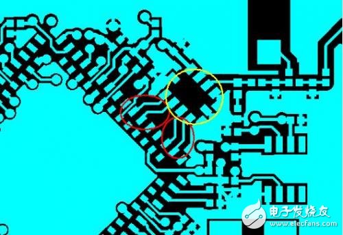
This circuit is a circuit of a high-performance RF chip and an integrated BALUN (the yellow part of the IC). Since there is no matching circuit between the main chip and the BALUN, this part is completely through the line width of the RF trace. And the impedance control of the differential signal to match, can not be debugged later by the peripheral device, so there are strict requirements for the trace of the differential part (as shown in the red part of the figure above), the quality of the trace and impedance control will directly affect the whole RF Part of the post-debugging indicators are good or bad, so the design requirements for the RF chip EVB board must be referenced at the beginning of the design, so that it can get twice the result with half the effort.
RF circuit layout needs to be countedIn the design process of many of our projects, design cost will be an important part of our design process. The cost of our RF circuit is mainly based on whether the peripheral circuit is built with separate components or integrated IC. Part of the use of integrated circuits will be more expensive than using separate devices, so here we mainly talk about what needs to be noted in the peripheral circuits of separate devices.
The following figure shows part of the circuit of a path in a design:
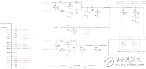
Since the periphery is a circuit built using capacitive inductors, the layout of this part of the circuit is more important on the premise that our board size requirements are getting smaller and smaller.
1. The RF parts should be placed on the same layer as much as possible. Try to avoid the RF traces from being punched to the other side. This layout is mainly to reduce the risk of RF index problems caused by PCB board punching.
2. Considering the integrity of the RF trace floor, if the large package is not guaranteed, try to use a small package to save more space and complete the floor.
3. Designed Circuits If there are multiple circuits of WLAN, BLE, and Zigbee, mutual interference and coexistence of multiple signals requires us to consider the layout of the traces at the beginning of the design, and try to make the layout and device placement safe. Distance reduces our uncontrollable requirements for later product performance.
Control the process to make the product performance in one stepAll the efforts in the early stage of circuit design are that the products made are a qualified product. For RF products, process control is particularly important. The following are simple:
1. PCB technology, RF board has strict requirements on PCB board and RF part trace impedance control. RF trace impedance 50 ohm and differential impedance 100 ohm requirements need to be confirmed by the PCB board factory whether the board factory can do it. Have done RF PCB board factory to play board.
2. The pre-commissioning is required for the brand of the material to be used, and the material of the commissioning material and the mass production must be the same.
3. For the PCB supplier requirements, the pre-development proofing and mass production ensure that the PCB manufacturers are consistent. If you want to import multiple PCB suppliers, you need to verify the RF specifications of the PCB boards provided by different manufacturers.
RF circuit design work requires R&D engineers to have a long-term work accumulation. There is no shortcut. An excellent RF engineer must have rich RF product development and debugging experience. This article is only for some of my work, there are more RF solutions. Good products come from accumulation, and good design comes from accumulation. !
In the field of motion control, Kassel servo drive has the advantages of flexible architecture design, open system platform, good communication connectivity, convenient configuration, easy maintenance and high system reliability. It has won trust in many fields and provided efficient Ac Servo Drive and Servo Motor for management and control integration, energy optimization and comprehensive management.
Servo Drive,Ac Servo Motor Driver,Servo Inverter,Servo Motors And Drives
Kassel Machinery (zhejiang) Co., Ltd. , https://www.kasselservo.com