1. One of the ten pitfalls of the operational amplifier - rail-to-rail
After the output voltage of the op amp couldn't reach the power rail, I decided to use a rail-to-rail op amp, thinking it would allow the op amp to finally reach the power rail. While initially happy with this decision, I later uncovered a hidden pitfall waiting for me:
Take a look at a company offering rail-to-rail op amp products: "High-speed (>50MHz) rail-to-rail op amps support lower supply voltages, closer power rail swings, and wider dynamic range." Do you notice it:
“Supports lower supply voltages, closer swings to the power rail, and a wider dynamic range.â€
“Closer to the swing of the power railâ€
“Closerâ€
“Closeâ€
...
Looking at the manual for a rail-to-rail op amp:

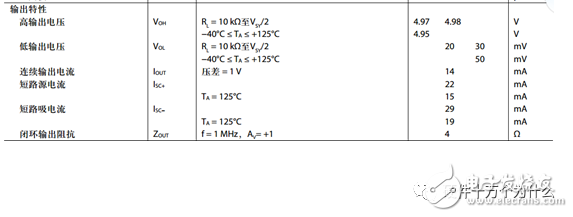
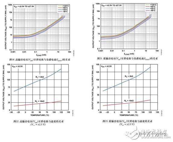
Why isn't the output voltage exactly 5V when connected to a 5V power supply?
The output stage of an op amp can be simplified to the following structure:
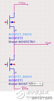
Since the MOS transistor has an on-resistance, when current flows through it, a voltage drop occurs. Thus, when the load is larger, the on-state voltage drop increases, making it harder for the output voltage to reach the rail.
Therefore, a rail-to-rail op amp is not entirely capable of making the output reach the power supply value. When using it, one must consider the relationship between the load and temperature (which affects the on-resistance's resistance) to determine how close the output can get to the rail.
2. The second pitfall of the op amp - non-negligible input bias current
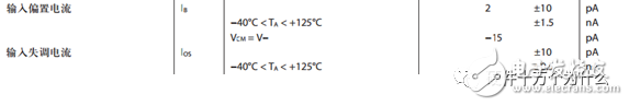
A voltage divider circuit was designed. In theory, inputting 1V should produce an output of 2V, but during testing, the output was always over 6.7mV. This was problematic since it was being sent to a 12-bit 3V range ADC, causing an error of over 600 counts.
The positive and reverse inputs of the op amp generated input bias currents due to TVS leakage current and the inherent input bias current of the transistor (since no two devices are exactly alike, the input bias currents at both inputs are not the same). These two bias currents formed a bias voltage with the external resistors and output to the back end, creating an error. Choosing a BJT-based op amp with a large input bias current can significantly impact the back-end error. As shown in the figure below, such an op amp is truly "awkward and hard to handle."

Assuming the input bias currents of the two inputs are the same:
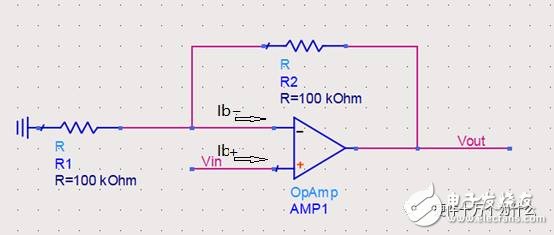
For the forward input, Ib+ brings the bias voltage close to 0, while for the inverting input, Ib- brings the bias voltage to 350mV (assuming Vout is grounded, equivalent to R1/R2). Therefore, a resistor needs to be added to the forward input to compensate for the error caused by the inverting input.
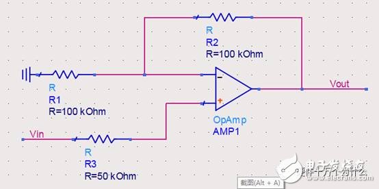
As mentioned earlier, the positive and negative input bias currents are not the same, and compensation can only reduce the offset voltage. The difference between the positive and negative input bias currents is also known as the offset current. When performing high-precision or small-signal sampling, a low-offset current op amp can be selected. Adding a compensation resistor introduces a new noise source, which should be carefully added.
The input bias current is one of the main errors of the op amp. In the following pitfalls, some error sources affecting the back stage are also introduced.
3. The third of the three holes of the operational amplifier - the rapid decline of PSRR
When I was a rookie engineer, I never considered PSRR in op amp design. Once I learned about PSRR, I began choosing op amps with higher PSRR based on cost control.
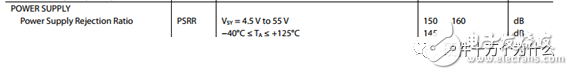
For example, this op amp has a PSRR of 160dB:
According to the calculation formula:

Even if the supply voltage changes between 4.5V and 5.5V, the effect on the op amp's output is only 10nV.
Unfortunately, this indicator refers to the DC change of the power supply voltage and does not include changes in the power supply voltage ripple. In the case of AC, this indicator will be greatly degraded. What is mentioned in the specification is only the DC change. The change of communication is shown in the figure below. Under normal circumstances, non-senior engineers tend to overlook this.
If the op amp circuit uses a switching power supply and decoupling and filtering are not done well, the input accuracy of the back stage will be greatly affected. Look at the AC PSRR of the same op amp.
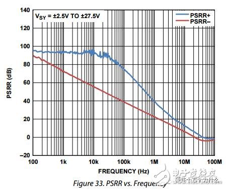
At a 500kHz switching frequency ripple, PSRR+ deteriorates to only 50dB. Assuming a ripple size of 100mV, the effect on the back stage will deteriorate to 0.3mV. For many small signal acquisition applications, this error is unacceptable. Therefore, some applications even make a low-pass filter at the op amp power inlet (noting the resistor power and resistor thermal noise).
4. The fourth of the ten pitfalls of the operational amplifier - the chaotic compensation capacitor
Once, an "old engineer" told me that adding a capacitor to the feedback circuit would prevent the circuit from oscillating. As soon as I read the word "chaotic," I was convinced. From then on, all my future circuits were combined with a small capacitor, making me feel professional.
Until one day, I wanted to amplify a 100kHz signal (luckily, the frequency wasn't too high, otherwise the voltage feedback op amp wouldn't work). Following experience, I added a capacitor, and... the signal became abnormal. ... Because, this capacitive feedback impedance dropped to less than 200Ω for a 100kHz signal, changing the amplification factor.
Of course, this isn't the main issue. The real question is: Do you really need a compensation capacitor?
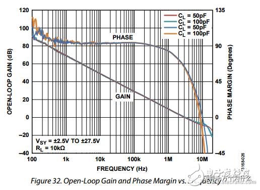
First, there's a pole inside the op amp (caused by RC low-pass), which causes a phase shift of up to -90°:
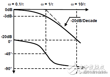
Adding another pole changes the phase again, increasing it to a maximum of 90°:
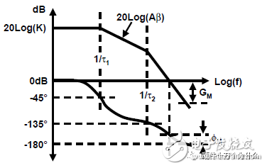
So, when the phase is -180°, what's the problem? That's the "chaos." Look at the gain of the voltage negative feedback op amp:
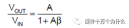
When the loop gain Aβ at certain frequency points equals 1 and the phase is -180°, then Vout/Vin becomes infinite and the circuit becomes unstable. Therefore, adding an external zero can cause the op amp to oscillate at certain frequency points, such as the distributed capacitance on the pins, as shown below:
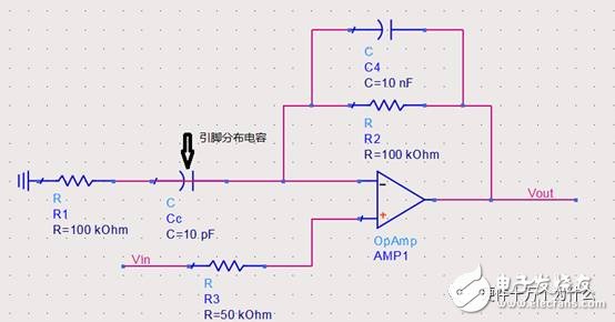
At this point, we add a capacitor, which is equivalent to artificially introducing a zero and pulling down the phase. However, this distributed capacitance is usually small, so the loop gain Aβ equals 1 at a very distant frequency, and the op amp works fine. Looking at the manual, the op amp itself is stable at 100kHz, with a phase margin of over 90°, so no additional compensation capacitors are needed.
Thus, for specific situations, we must analyze them in detail and not blindly follow the advice of the "old engineer."
5. The fifth of the ten pitfalls of the operational amplifier - the common mode input range of the op amp
I once encountered a problem where the preamplifier amplified the signal and then passed it to the ADC, with the signal into the ADC ranging from 0.3V to 1.5V. It seemed like a simple circuit, but the actual measurement showed that when using a single 5V power supply op amp, some boards outputting around 1.5V had outputs that did not completely follow the input values, being lower than expected. The 1.5V signal worked fine, but it wasn't right when it got close.
Of course, this issue was discussed in the hardware team meeting. The final conclusion was: "There's a problem with this op amp. We're looking for manufacturers to replace it, but since we're from xx company, they don't care about us, so let's switch to another company's op amp." Unfortunately, after picking up a new op amp, we still couldn't find the root cause of the problem. Luckily, we didn't fully understand the principle, and we happened to choose a working op amp.
Looking at an indicator of this op amp, the op amp's common-mode input range:
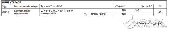
The op amp's common-mode input range is an interval of the op amp's input voltage. It characterizes the interval in which the op amp can operate linearly. That is, when the input voltage common-mode value is within this interval, the output voltage can change linearly with the input voltage.
For the follower circuit, due to negative feedback, the positive-phase input terminal voltage and the negative-phase input terminal voltage are basically the same value, and the common mode input range is -0.1V to the 5V power supply at 1.5V. Therefore, when the input voltage is around 1.5V, there is a case where the op amp cannot follow normally.
Why can't it follow? Let's look at a triode amplifier circuit, which is also part of the op amp, for illustration.
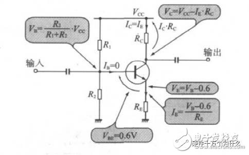
When the input Vb changes, Ie changes accordingly with Vb, causing Vc to change, which is followed. If Vb continues to increase to Vc=Vcc-Ie x Rc, the calculated value is negative, but in fact Ie x Rc cannot exceed Vcc. At this time, the amplifying circuit reaches saturation or even the current is inverted, resulting in fixed or cut output voltage. Peak or reverse, etc.

The castings produced by the Silica Sol Casting process have high dimensional accuracy and can reach the CT4-8 level specified in GB/6414-1986. The surface roughness value is low, which can reach RA0.8-6.3μm. No machining; the silica sol casting process also produces castings with more complex geometries
Investment Casting,Lost Wax Casting,Steel Investment Casting,Stainless Steel Investment Casting
Tianhui Machine Co.,Ltd , https://www.thcastings.com