Ultrasound has long been a critical technology in the medical equipment field, known for its strong penetration and high detection sensitivity. However, its applications are no longer limited to healthcare; it is now widely used in industries such as aerospace and metallurgy. Today’s ultrasonic flaw detectors employ either analog or digital non-destructive testing techniques. With advancements in computer technology, microelectronics, and digital signal processing, traditional analog systems are gradually being replaced by more advanced digital ones.
The echo signals from ultrasonic waves are high-frequency signals, with center frequencies reaching up to 20 MHz. Commonly used ultrasonic probes typically operate within a frequency range of 2.5 to 10 MHz. Digitizing such high-frequency signals requires an analog-to-digital (A/D) conversion system that can handle high-speed sampling. According to the Shannon sampling theorem and Nyquist criterion, the sampling rate should be at least twice the highest frequency of the input signal. In practice, to ensure data accuracy, it is common to sample 7 to 10 times per cycle. Some systems require even higher sampling rates, but current A/D solutions often fall short in terms of reliability, power consumption, speed, and precision. The development of large-scale integrated circuits has opened new possibilities for high-speed, high-precision, and low-power ultrasound signal acquisition.
This paper presents a 100 MHz sampling-rate ultrasonic acquisition module, which uses an FPGA to compress and buffer the sampled data. The design focuses on key technologies, particularly the A/D conversion unit and data buffer.
**1. Principle of Digital Ultrasonic Flaw Detector**
Figure 1 shows the block diagram of a digital ultrasonic flaw detector. It includes components such as the ultrasonic transmitter, receiver, signal conditioning unit, A/D converter, data buffer, data processing unit, waveform display, and system control. This paper mainly discusses the high-speed data acquisition technologies involved in these systems, focusing on the A/D and data buffer units.
**2. High-Speed, High-Precision Sampling Hardware Structure**
**2.1 Block Diagram of the Data Acquisition Module**
As shown in Figure 2, the data acquisition module consists of a high-speed A/D converter, an FPGA, clock circuit, reset circuit, and power supply. The A/D handles signal acquisition and conversion, while the FPGA manages control, compression, and buffering.
**2.2 Introduction to AD9446**
The AD9446 is a 16-bit ADC capable of sampling at up to 100 MSPS. It features a built-in sample-and-hold amplifier and reference voltage source. It supports differential input, offering excellent noise rejection. The device can operate in CMOS or LVDS mode, and its output format is configurable. In PCB design, careful attention must be paid to power supply isolation, ground layout, and reference voltage stability to minimize noise interference.
**2.3 FPGA Implementation for Acquisition Control, Data Compression, and Buffering**
The FPGA, specifically the Xilinx Spartan3E series (XC3S500E), controls the acquisition process, performs data compression, and manages data buffering. It uses a FIFO for data storage and ensures efficient communication with the microprocessor.
**2.3.1 Data Acquisition Control**
The AD9446 operates based on clock timing, with sampling initiated on the rising edge of the first clock pulse. The DCM within the FPGA helps manage clock signals, ensuring synchronization between the FPGA and the A/D converter.
**2.3.2 Data Compression**
To reduce data volume without losing essential signal information, the system only retains the maximum value from each set of samples. This compressed data is then sent to a latch, and the microprocessor processes it accordingly.
**2.3.3 Data Buffering**
An internal FIFO in the FPGA stores the compressed data, allowing for efficient data transfer to the microprocessor. The size of the FIFO can be adjusted based on the available FPGA resources.
**3. Conclusion**
This paper presents a high-performance data acquisition module based on the AD9446 ADC, integrating control, compression, and buffering functions. It improves system reliability, simplifies hardware, and enables future upgrades. The use of high-speed, high-precision A/D conversion ensures accurate data acquisition, while FPGA-based preprocessing enhances data handling efficiency for the microprocessor.
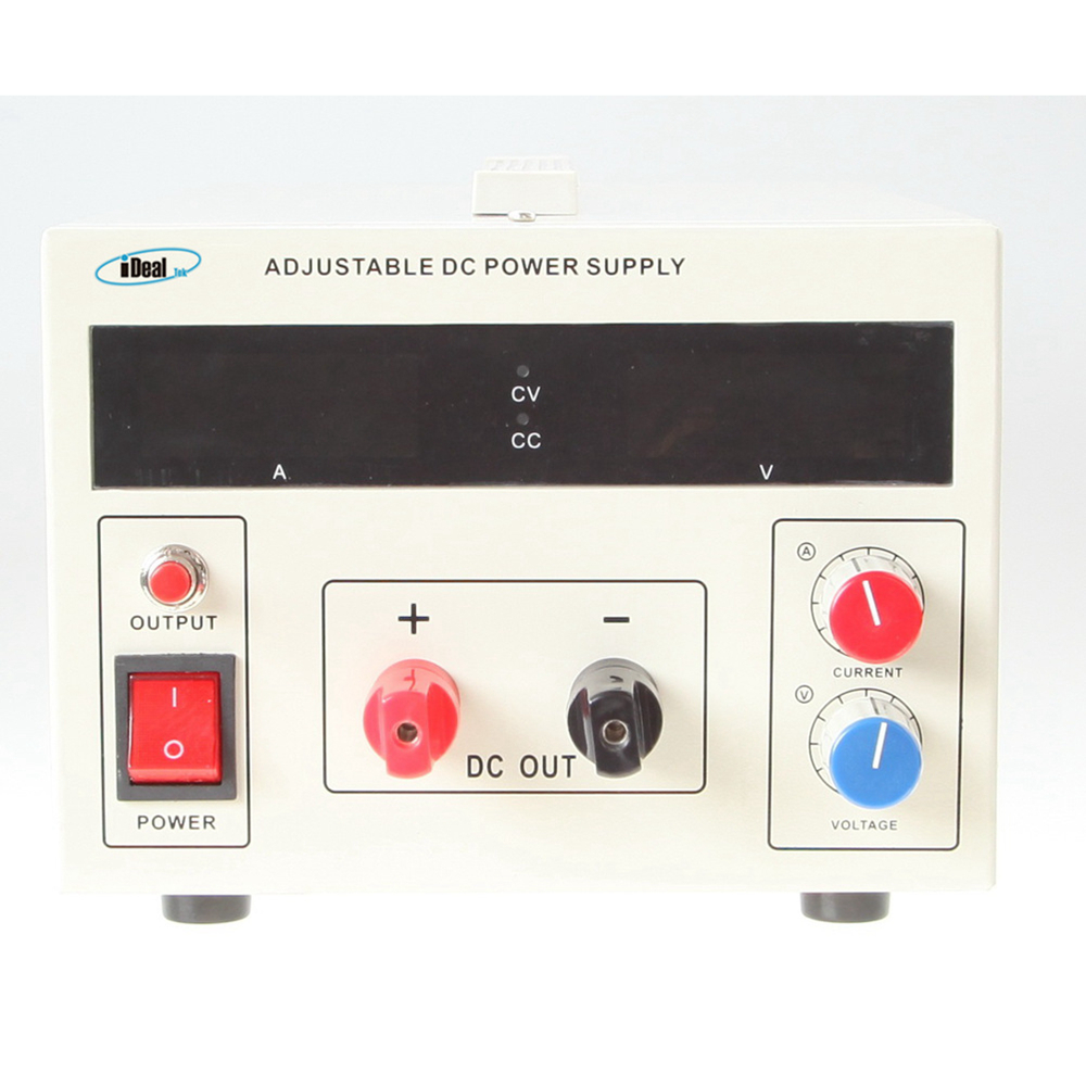
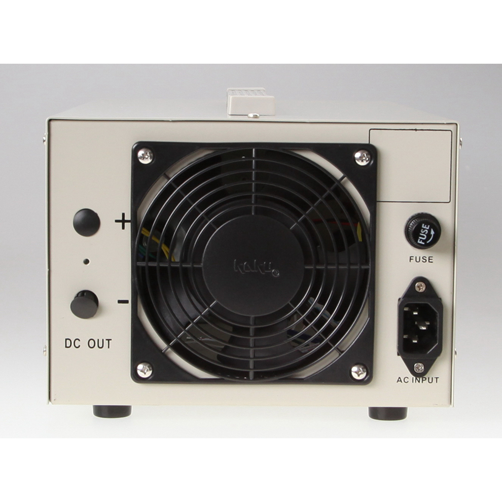
Benchtop DC Power Supplies
SMP series Bench DC Power Supplies are economical, MOSFETs-based, high switching speed, high power density desktop DC power supplies with output power covering 300W ~ 6KW, and maximum voltage up to 800VDC.
Compared with IGBT-based DC switching power supplies, MOSFET-based switching power supplies have a higher switching frequency, making this series Benchtop DC power supplies can use smaller semiconductor devices and LC filter units while ensuring low ripple, high precision, and fast response characteristics of the Benchtop Laboratory Power Supplies DC output. Which gives more space to use a smaller chassis size at the same output power, resulting the high-power density feature of this series Benchtop AC DC power supplies.


The main design purpose of this series of Bench AC-DC power supplies is to fulfill the needs of small laboratory test, precise experiment and universities.
At present, this series of Bench AC DC power supplies below 1KW adopts desktop chassis to match laboratory applications, they are mainly used in LED testing, small electroplating, heating of new materials, electrical component testing and other applications.
Bench DC Power Supplies, Desktop DC Power Supplies, Bench Laboratory Power Supplies, Benchtop AC DC Power Supplies, Bench AC-DC Supplies
Yangzhou IdealTek Electronics Co., Ltd. , https://www.idealtekpower.com

