Ultrasound has always been a critical technology in the medical equipment field, known for its strong penetration and high detection sensitivity. However, its applications have expanded far beyond healthcare, now being widely used in aerospace, metallurgy, and other manufacturing industries. Today, ultrasonic flaw detectors are available in both analog and digital forms. With the advancement of computer technology, microelectronics, and digital signal processing, traditional analog ultrasonic flaw detectors are gradually being replaced by more advanced digital versions.
The echo signals from ultrasonic waves are high-frequency signals, with center frequencies reaching up to 20 MHz. The frequency range of commonly used ultrasonic probes is typically between 2.5 MHz and 10 MHz. Digitizing such high-frequency signals places significant demands on the analog-to-digital (A/D) conversion circuit. According to the Shannon sampling theorem and Nyquist criterion, the sampling frequency must be at least twice the highest frequency of the input signal to avoid distortion. In practice, to ensure data accuracy, it is common to sample 7 to 10 times per cycle. Some systems require even higher sampling frequencies. Existing A/D circuits often face issues with reliability, power consumption, speed, and precision, making them unsuitable for certain applications. The development of large-scale integrated circuits has enabled high-speed, high-precision, reliable, and low-power solutions for ultrasonic signal acquisition.
This paper presents a 100 MHz sampling rate ultrasonic acquisition module that compresses sampled data using an FPGA to buffer the information. The design focuses on key technologies in digital ultrasonic flaw detectors, particularly the A/D conversion and data buffering units.
**1. Principle of Digital Ultrasonic Flaw Detector**
Figure 1 shows the block diagram of a digital ultrasonic flaw detector. It generally includes an ultrasonic transmitter, receiver, signal conditioning unit (such as amplification, filtering, and detection), A/D converter, data buffer, data processing unit, waveform display, and system control and I/O functions. This paper mainly discusses the high-speed acquisition techniques involved in these systems, focusing on the A/D and data buffer modules.
**2. High-Speed, High-Precision Sampling Hardware Structure**
**2.1 Block Diagram of the Data Acquisition Module**
Figure 2 shows the hardware block diagram of the data acquisition module, consisting of a high-speed A/D converter, FPGA, clock circuit, reset circuit, and power supply. The A/D converter handles signal acquisition and conversion, while the FPGA manages control, compression, and buffering. The following sections describe the A/D converter and FPGA in detail.
**2.2 Introduction to AD9446**
The AD9446 is a 16-bit ADC with a maximum sampling rate of 100 MSPS, featuring a built-in high-performance sample-and-hold amplifier and reference voltage source. It supports differential input, offering excellent rejection of common-mode and even signals. The AD9446 can operate in CMOS or LVDS mode, with mode selection controlled via logic pins. Its digital output can be set to either binary or two's complement format. During PCB layout, care must be taken to separate analog and digital grounds, match differential input lines, and use a precise reference voltage to reduce noise.
**2.3 FPGA Implementation for Acquisition Control, Data Compression, and Buffering**
The FPGA, specifically the Xilinx Spartan3E series (XC3S500E), is responsible for data acquisition control, compression, and buffering. It offers powerful I/O resources and flexibility for various applications.
**2.3.1 Data Acquisition Control**
The AD9446 operates based on clock signals, with sampling and data output controlled by the rising edge of the CLK signal. The Digital Clock Manager (DCM) within the FPGA allows for clock division, multiplication, and phase adjustment, ensuring proper synchronization with the AD9446. VHDL code is used to implement the clock output after DCM configuration.
**2.3.2 Data Compression**
Data compression is crucial for handling high-frequency sampling. The FPGA captures only the maximum value during each sampling interval, discarding others. This method maintains the essential characteristics of the ultrasonic echo while reducing data volume. The compressed data is stored in FIFO for later processing.
**2.3.3 Data Buffering**
To address rate mismatch between front-end acquisition and back-end transmission, an 8K × 16-bit FIFO is implemented within the FPGA. Compressed data is stored in the FIFO, and the microprocessor reads it through interrupts. The FIFO is generated using a core generator, requiring minimal control logic.
**3. Conclusion**
The designed data acquisition module based on AD9446 successfully implements control, compression, and buffering functions. It simplifies the hardware, improves system reliability, and facilitates future upgrades. The high-speed, high-precision A/D converter meets the requirements of digital ultrasonic testing, while FPGA preprocessing enhances data accessibility for the microprocessor.
High Voltage Linear Power Supplies
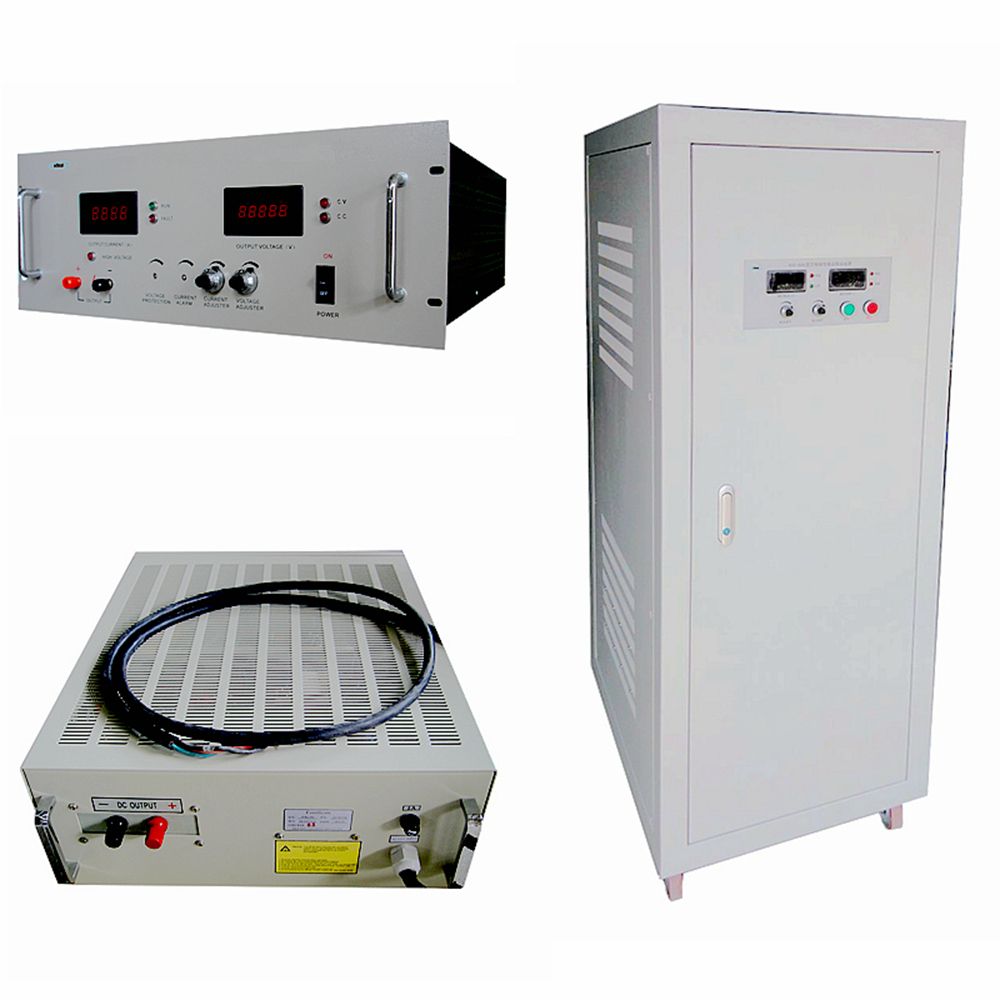
HVLP series Linear High Voltage Power Supplies are High-voltage DC Power Supplies that achieve AC/DC conversion through power frequency transformers and transistor loop control. Compared with switching high voltage power supplies, linear high-voltage power supplies have higher stability, higher accuracy, and lower output ripple. And the most important, because of the use of the power frequency AC/DC conversion principle, the linear power supply has no high-frequency radiation interference, and it is especially suitable for use in places with restrictions on EMC and EMI.

The HVLP series Linear Power Supplies have a wide range of output specifications, the output power ranges from 1KW to 400KW, and the output voltage can reach up to 50KVDC, and accept customization.
The whole series linear power supply adopts industrial-grade metal chassis, pure copper AC/DC multi-insulation high-voltage transformer with varnish treatment, high-reliability multi-transistor filter loop, ensuring the power supplies can run for a long time at full load with high stability, high accuracy, and ultra-low ripple electronic characteristics, equipped with a complete protection circuit, which can better ensure the reliability of the linear power supply itself and the safety of the customer's load.
The output voltage and current can be adjusted by the 10-turn potentiometer with scale and lock on the front, equipped with 4 1/2-digit high-resolution LED meters for output value reading, and RS communication interface can also be added for remote control and monitoring of linear power supplies.
This series of linear high voltage power supplies are mainly used for gas discharge, high-voltage electronic tubes, and can also be applied for other electronic components burn-in test.
Because the output this power supply has HV, the output MUST be connected to the chassis for fixed grounding to ensure the personal safety of the user.
High-voltage Linear Power Supplies,Linear High Voltage Power Supplies, HV Linear Power Supplies, Linear HV Power Supplies, Linear HVPS
Yangzhou IdealTek Electronics Co., Ltd. , https://www.idealtekpower.com
