introduction
At present, energy-saving lamps are the most widely used electric light source. Although the electronic energy-saving lamps are no longer at the forefront of the lighting industry due to the sudden emergence of semiconductor lighting, its development potential is unquestionable. In the field of general lighting, LED light sources cannot completely replace energy-saving lamps for a long time.
In the face of the severe situation of global energy shortage, dimming technology has attracted more and more attention in the field of lighting. It is an energy-saving measure for users to dim the energy-saving lamps according to actual needs. There are several options for dimming energy-saving lamps. Among them, Triac traditional dimmer is a low-cost simple analog dimming solution. The use of a Triac dimmer for dimming an energy-saving lamp based on electronic ballasting of a control IC has the basic premise that the ballast control IC must have a dimming function. There are many dimmable energy-saving lamp control chips, and the L6574 produced by ST is one of the representative devices.
1 Introduction to Dimmable Ballast Controller L6574
The L6574 is available in a 16-lead SO and DIP package with pinouts as shown in Figure 1.
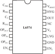
Figure 1 Pinout of the L6574
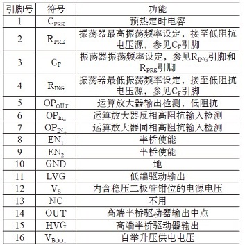
Table 1 lists the pin functions of the L6574.
Table 1 Pin Function of L6574
The working principle of L6574 can be illustrated by Figure 2.
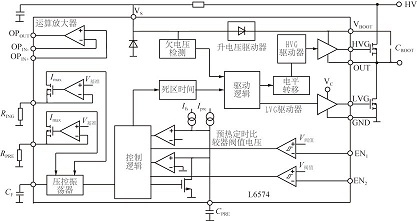
Figure 2 L6574 working principle diagram
The upper and lower drivers of the L6574 are designed to drive an external half-bridge switch (MOSFET). The L6574 contains a voltage controlled oscillator and a filament preheat timing comparator. When the IC oscillator is started, the preheating frequency fPRE is first output. The value is set by the external resistor RPRE on IC pin 2, the external resistor RING on pin 4, and the external capacitor CF on pin 3. The calculation formula is :
The filament heating time tPRE is set by the external pin capacitance CPRE of IC pin 1, and can be calculated according to formula (2):
After the warm-up is over, the frequency is scanned from the fPRE to the low normal operating frequency fING. When the frequency passes through the resonant frequency of the load LC network, a high voltage pulse is generated across the lamp capacitor to illuminate the lamp. The lighting time tIGN is 10% of the warm-up time, ie:
After the lamp is ignited, it operates at the operating frequency fING. fING can be calculated according to formula (4):
The L6574 includes an op amp with high input impedance, wideband, large common-mode range, and low output impedance for closed-loop control of the light current and dimming.
The L6574 pins EN1 and EN2 are internal comparators with a threshold voltage of 0.6V. They can recognize short pulses from the input terminal of less than 200ns. They protect the overvoltage or filament from being blown and the lamp is not connected. When the IC pin EN1 is high, the IC is forced to enter the shutdown mode and the oscillator circuit stops oscillating. When the pin EN2 inputs a high level voltage, the IC re-enters the startup sequence.
The turn-on voltage on the L6574 pin VS is 10.2V, and the undervoltage closes the threshold at 8V. The VS voltage is clamped to the 15.6V level by the internal Zener diode.
2 Typical dimmable ballast circuit based on L6574
A typical 58W dimmable ballast half-bridge inverter and resonant output stage circuit based on L6574 is shown in Figure 3.
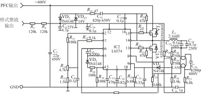
Figure 3 58W ballast circuit based on L6574
According to the international standard IEC61000-3-2, since the lamp power is >25W, power factor correction (PFC) must be used. The front end of the circuit of Figure 3 is an active PFC boost converter based on L6561, which provides 400V DC bus voltage for the ballast part shown in Figure 3, and guarantees the system input power factor of 0.99, AC input current total harmonic Distortion (THD) <10%.
The start resistors R3 and R4 are connected to the bridge rectifier output instead of the DC 400V bus, which allows R3 and R4 to withstand lower voltages. After IC2 is started, as long as the half bridge starts to produce output, the high frequency voltage is coupled by C11, VD2 rectifies and C6, C20 filter, and is added to IC2 pin 12 to supply power to IC2. The voltage VS on pin 12 is clamped at 14V by VDZ1.
When the potentiometer R14 on IC2 pin 2 is adjusted to the maximum, the resistance value is 4.7kΩ. Therefore, RPRE=R13+R14+R15=100kΩ+4.7kΩ+1.5kΩ=106.2kΩ. The grounding resistance R19=RING=100kΩ on IC2 pin 4, the capacitance C13=CF=470PF on pin 3, and the capacitance C14=CPRE=0.82μF on pin 1 are calculated according to formulas (1)~(4):
fPRE = 60 kHz, tPRE = 1.2 s, tIGN = 0.12 s, fING ≈ 30 kHz.
If the lamp is not connected, the voltage VS on pin 12 of IC2 is applied to pin 8 (EN1) via resistors R26 and R27. The CMOS comparator will force IC2 into shutdown mode and the half-bridge circuit is turned off. After the filament is warmed up, if the lamp cannot be illuminated, an additional voltage will be generated across resistor R30, rectified by VD4 and C15 filtered, applied to IC2 pin 9 (EN2), and IC2 re-enters the preheat and lighting procedure.
R25 connected to the MOSFET source under the half bridge is the current sense resistor, and the current sense signal on R25 is applied to pin 6 (OPIN_) of IC2 via R33. VD3 and R18 are connected between pin 5 (OPOUT) and pin 4 (RING) of IC2. The function of VD3 is to prevent the switching frequency from being lower than the frequency set by R13. When the lamp ignites, the voltage on R25 increases and the op amp in IC2 begins to control the lamp current in a closed loop. By adjusting the resistance value of R14, the switching frequency can be changed to adjust the lamp current and lamp power to realize the dimming function.
3 Triac dimmer dimming implementation
1) Ordinary electronic ballasts use Triac dimmer to dim light and flashing lights
An incandescent lamp is a purely resistive load that dims an incandescent lamp with a conventional Triac dimmer. The Triac can be turned on at any point in the AC input sine wave until it is turned off when the sinusoidal voltage approaches zero. Therefore, incandescent lamps can achieve smooth dimming from almost 0% to 100%.
The situation of the electronic ballast is completely different from that of an incandescent lamp. The Ttiac dimmer is connected to the input of the bridge rectifier (or EMI filter), as shown in Figure 4.
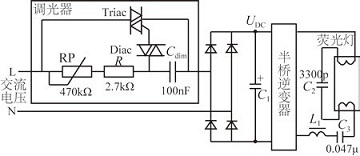
Figure 4 Triac dimmer connected to the bridge rectifier input
We do not consider the case of dimmer access first. Since the rectifier diode has unidirectional conductivity, it is turned on only when it is forward biased. Only near the peak of the AC input voltage, the AC voltage will be higher than the voltage on the storage capacitor C1, and the diode will have current. Therefore, the AC input current is no longer sinusoidal, but a high amplitude spike, as shown in Figure 5. In the half cycle of 10ms, the diode conduction time is only about 3ms, and the corresponding conduction angle is only about 60°.
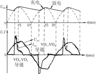
Figure 5 AC input voltage, input current and rectified and filtered output voltage without considering the dimmer
When the dimmer used in the incandescent lamp is connected to the electronic ballast input (see Figure 4), the Triac will only be triggered to conduct when the AC input voltage is greater than the voltage across the smoothing capacitor C1. Although the fluorescent lamp can be dimmed to a certain extent, the light will flicker and cannot be practical.
2) Triac dimming solution
In order to achieve smooth dimming of the electronic ballast with an incandescent thyristor dimmer, the lamp flicker is eliminated, and the solution is shown in FIG. 6.
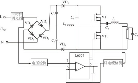
Figure 6 Triac dimming solution block diagram
In addition to sensing the lamp current feedback, the AC input voltage after the dimmer is sensed and the sense signal is input to the non-inverting terminal of the L6574 op amp as the reference control voltage. The voltage detection circuit is very simple and can be sampled with a resistor divider and then a rectified filter network.
Detecting the voltage after the dimmer actually controls the knob position of the dimming potentiometer (ie, the conduction angle of the Triac).
In order to achieve smooth dimming, a single-stage PFC circuit must be added to the ballast circuit. In Figure 6, C2, C3, VD5, VD6, L2, C3 and power MOSFETs VT1, VT2 are single-stage PFC circuits.
To illustrate the operation of a single-stage power factor correction (PFC) circuit, we assume that the dead time of the switch (ie, the time interval between VT1 turn-off and VT2 turn-on) is negligible; the duty cycle of VT1 and VT2 is 50. %; The voltage across capacitors C2 and C3 is constant during one switching cycle. Figure 7 shows the waveform of current iL2 through inductor L2 during a switching cycle.
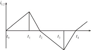
Figure 7 Single Switch Cycle Inductance L2 Current
iL2 can be divided into 4 stages.
T0~t1: This period L2 is charged. At t=t0, VT1 is turned on, VT2 is turned off, C2 is charged to L2 through VD5 and VT1, and iL2 is linearly increased. At time t1, VT1 is turned off, VT2 is turned on, and iL2 reaches a positive peak.
The t1 discharge (voltage is UC2-UC1), iL2 linearly decreases. At time t2, iL2=0, VDS2 is turned off, and VT2 is turned on.
T2
T3
In fact, the single-stage PFC circuit is composed of two boost circuits, iL2 operates in both directions and operates in a critical discontinuous mode. After adding a single-stage PFC circuit, the AC input current can continuously pass through the diode in the rectifier. The Triac can be turned on almost at any time from 0° to 180° until the AC sinusoidal voltage approaches zero. Expanded the dimming range.
For the circuit shown in Figure 6, if the load is a 20W energy-saving lamp, and the AC input voltage range is 180 ~ 260VAC, the lowest switching frequency is 45kHz, L2 = L1 = 2.8mH, C1 = 10μF, C4 = 0.1μF, C5 = 5.6nF, VT1 and VT2 are STD4NK50 MOSFETs, and the dimming characteristics at 220V/50Hz are shown in Figure 8.
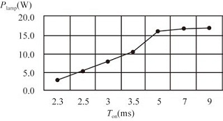
Figure 8 Dimming characteristics at 220Vac and 50Hz
Among them, Ton is the conduction time of Triac in the AC line half cycle (10ms), and Plamp is the measured lamp power. As can be seen from Fig. 8, as the Triac conduction time increases, the lamp power increases correspondingly, thereby increasing the brightness of the lamp. Conversely, the shorter the Ton, the smaller the lamp power and the darker the light.
Figure 9 shows the AC input voltage and current waveforms. It can be seen from the figure that although the AC current has a peak near its peak, the Triac can be turned on at any point, and the rectifier diode in the half cycle is turned on almost from 0° to 180° without using a single The conduction angle of the PFC circuit is only 60° (see Figure 5), and the line power factor is above 0.9. Of course, the main purpose of adding a single-stage PFC circuit is to enable Triac to be turned on at any point between 0° and 180°.
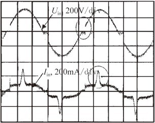
Figure 9 Input voltage and current waveforms
4 Conclusion
The L6574 is a dimmable fluorescent lamp AC electronic ballast controller. Based on the L6574 ballast, a single-stage PFC circuit is added, and the input voltage and the average current of the lamp are sensed by the operational amplifier in the L6574. With the dual functions of frequency modulation and voltage regulation, the traditional incandescent lamp Traic dimmer can be used. , to achieve dimming from 20% to 100%, making it a great advantage in energy saving.
Offer Gift Shop Pos,Gift Shop Pos Software,All In One Touch Pos From China Manufacturer
Fly through transactions
Gmaii Gift Shop Pos System can be laid out exactly how you want for maximum speed. Faster transactions make for shorter lines (and happier customers).
Maximize your profit
Gmaii Gift Shop Pos System not only tracks your gift shop's inventory automatically, it even helps you understand which items are driving your sales and which ones it's time to replace.
Mini taxis for sale in a gift shop
Manage your gift shop
With Gmaii Gift Shop Pos System, you know everything from your sales in real time, to your staff's clock-in times, and much more, all from your computer or smartphone.
Increase repeat business
What's better than a one-time customer? A repeat one! Gmaii Gift Shop Pos System has built-in marketing tools to keep your gift shop at the forefront of people's minds.
Customers in line at a gift shop
Versatile Gift Shop POS: The Bliss Way
Bliss in Boulder, CO used Gmaii Gift Shop Pos System to greatly speed up transaction times, grow profit margins, and maximize profits.
Gift Shop Pos System
Gift Shop Pos,Gift Shop Pos Software,All In One Touch Pos,Pos System Software
Shenzhen Gmaii Technology Limited , https://www.gmaiipos.com