Abstract: The MAX1460 is a digital-sensor signal processor (DSSP) implemented in fine-geometry mixed-signal CMOS technology. Though opTImized for the calibraTIon and the temperature compensaTIon of piezoresisTIve pressure sensors, the MAX1460 offers powerful performance in applications where the input signal is very small (mV range) and the offset, span, and temperature coefficients of offset and span are in need of correction. This app note describes the MAX1460 sensor signal conditioner in great detail.
The MAX1460 is an ASIC digital-sensor signal processor (DSSP) implemented in fine-geometry mixed-signal CMOS technology. This IC includes a high-resolution 16-bit sigma-delta analog-to-digital converter (ADC), a high- performance analog front end, a full 16-bit mathematical processing engine, and a fine-resolution 12-bit digital-to-analog converter (DAC) for signal output. Its key feature is a small and power-efficient digital signal processor (DSP ).
Though optimized for the calibration and the temperature compensation of piezoresistive pressure sensors, it offers powerful performance in applications for which the input signal is very small (mV range) and the offset, span, and temperature coefficients of offset and span are in need of correction (Figure 1).
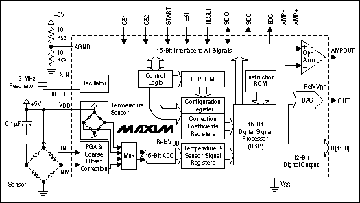
Figure 1. This drawing combines a block diagram and an application schematic for the MAX1460 signal conditioner.
Calibration and compensation coefficients are stored in an internal 128-bit EEPROM. The integrated DSP then calculates the compensation correction using these coefficients, the 16-bit digitized sensor signal, and the digitized temperature data. All corrections are performed in the digital domain. The conditioned output is then presented externally as a 12-bit digital word and (via the internal 12-bit DAC) as a ratiometric analog voltage proportional to the supply voltage.
The uncommitted op amp can be used to filter the analog output or to implement a 2-wire 4-20mA transmitter. Such built-in functionality enables the MAX1460 to support automotive, industrial, process, and aerospace applications, yielding total accuracies within ± 0.5 % (typical) of the sensor's inherent and repeatable error band over temperature. This residual error mainly includes sensor nonlinearity in response to pressure and temperature nonlinearity errors higher than second-order.
The MAX1460 digitizes the sensor signal, mathematically adjusts the signal for temperature effects, and converts the result back to an analog signal (and also outputs the digital result directly). The new feature that separates this architecture from previous schemes accomplished with CPU circuits is the presence of precision analog and digital functions on a single piece of silicon. Also integrated is the temperature measurement, which is ratiometric to the supply voltage. Everything is accomplished within the sensor assembly's final package and with supply currents below those of a conventional-circuit approach .
For the sensor signal and temperature digitization process (Figure 2), an important requirement is the sensor output's initial or coarse-offset adjustment. Because piezoresistive transducers (PRTs) typically have large offsets, it is necessary to add an analog signal offset to bring the differential sum to nearly zero. A 3-bit-plus-sign DAC generates the coarse-offset signal, which ranges from nearly zero to more than ± 150mV.
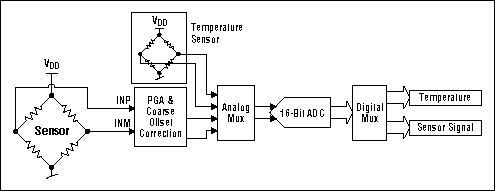
Figure 2. Detail from Figure 1: digitizing the temperature and pressure-sensor signals.
In addition, the low-level PRT signal must be amplified to make maximum use of the ADC resolution. This is accomplished with a fully differential programmable gain amplifier (PGA) in which four gain settings span the optimum values ​​for today's PRT devices: 46, 61, 77, and 93V / V. The coarse-offset-compensated signal is multiplied by one of these gain factors to enable a maximum output-voltage swing from the PGA without saturating to either supply rail. This nonsaturating condition applies to all pressure ranges over all temperature ranges.
The differential, 16-bit delta-sigma ADC is preceded by an analog multiplexer and followed by a digital multiplexer. Simultaneous channel selection in these multiplexers routes the coarse-offset, amplified differential signal from the PGA to the ADC, and (when the conversion is complete) routes the digital ADC result to the sensor-signal register.
Coincident with multiplexing the ADC digital output to the temperature register, the differential temperature signal (derived from an integrated temperature-sensitive bridge made from a combination of n-well and polysilicon resistors) is multiplexed to the ADC. The resulting digitized value has a sensitivity of 0.0038 ° C / LSB and a linearity error of only 1.3 ° C. The digitized-temperature output value corresponding to the ADC's zero output is set to approximately 25 ° C.
Before compensation, the offset and span of a piezoresistive pressure sensor exhibit variations with temperature that can be greater than 10%. Also visible in these curves is a slight nonlinear curvature indicative of second-order effects. Compensation of these temperature errors requires use of a common temperature-linearization equation:
DOUT = Gain × (1/2 + G1 × T + G2 × T²) × (Signal + Of0 + Of1 × T + Of2 × T²) + DOFF (1), where
Evaluation of this equation requires addition and multiplication. Though not explicitly obvious from the equation, a third arithmetic operation (negation) is also required. To maintain the highest level of precision, all arithmetic operations should be performed at the resolution of the input signal, which in this case is 16 bits.
The DSSP is a reduced-instruction-set-computer (RISC) processor (Figure 3) whose 16 instructions are designed to perform the mathematical operations required in solving the linearization equation above. In addition, its register-based architecture is limited to 16 registers and 16 ports. The ports are special-function 16-bit I / O locations for auto-loading the compensation coefficients from EEPROM, accessing the ADC results, and outputting data to the DAC. The DSP processing engine is 16 bits wide, as are all of the registers.
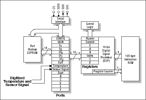
Figure 3. This block diagram details the architecture of the digital-sensor signal processor internal to the MAX1460.
The digitized temperature and sensor signals arrive in the DSSP's port space as soon as an ADC conversion is completed. Then, the linearization and compensation coefficients of the linearization equation are loaded into predefined ports from the port shadow EEPROM memory. In this way, the DSP can perform 16-bit operations from port data using any of the 16 registers and transfer the result to a port such as DOUT.
Port DOUT has a hardwired operation in which it directly drives the 12-bit parallel digital output and the internal 12-bit DAC. When the DSP has completed one iteration of the linearization equation, the result is placed in port DOUT. Thus, the equation result is immediately applied to the digital output pins and to the DAC for conversion to an output-signal voltage.
Ports B through F are used as general-purpose working ports for holding the intermediate calculations necessary in evaluating the linearization equation. The port CONFIG contains configuration settings for the PGA and the coarse-offset DAC and control functions governing the MAX1460's operating modes.
The DSP instructions are stored in a read-only memory (ROM) that is one byte wide (8 bits) and 128 bytes long. Each instruction contains information regarding which register or registers to operate on and what the operation should be. The instruction- byte format is shown in Figure 4, and the instruction set is shown in Table 1. The "X" register referred to in each instruction can be any of the 16 registers shown in Table 2.
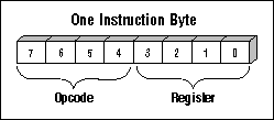
Figure 4. The DSSP instruction bytes have this structure.
Table 1. The RISC DSP Instruction Set (op-code portion)
Table 2. The RISC DSP Instruction Set (register portion)
Although a complete instruction code for the linearization calculation is not shown, two subroutines are offered: one for the squaring operation (Figure 5) and the other for the multiplication operation (Figure 6).
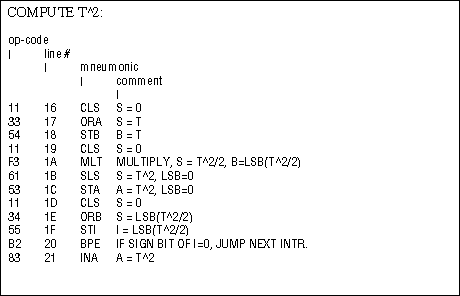
Figure 5. In evaluating the linearization equation, this code computes T².
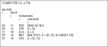
Figure 6. In evaluating the linearization equation, this code computes G1xT / 2.
The result of calculating the linearization equation is output in separate analog and digital formats. To indicate that a new result is available, a 12-bit parallel digital output is provided along with an end-of-conversion (EOC) signal. The EOC also loads the 12-bit data into a 12-bit delta-sigma DAC to generate the analog signal. Necessary filtering of the DAC output is accomplished with an integrated op amp (Figure 7).
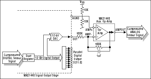
Figure 7. The MAX1460 provides a parallel digital output and (via a DAC) an analog output, filtered here by an external op-amp circuit.
The entire linearization equation shown in equation 1 is calculated after two ADC conversions are completed. The first conversion updates the sensor-signal port data, and the second updates the temperature port data. The equation calculation is completed in one pass through the 128-byte instruction ROM. At the end of the execution cycle, in which the digital and analog outputs have been updated, the DSP returns to the top of the instruction ROM and awaits completion of two more conversions.
The MAX1460 achieves accuracy in excess of 0.5%. To calibrate the sensor assembly (comprising the MAX1460 and the transducer element), you measure the assembly output at three temperatures and two sensor excitations, substitute each data item in the characteristic equation, and solve the resulting six equations in six unknowns. For a piezoresistive transducer, nonlinear span and offset errors exceed 8% and 3%, respectively. After compensation, its sensor output has span and offset errors less than ± 0.05% (Figure 8).
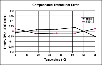
Figure 8. After compensating the sensor, span and offset errors are less than ± 1.5%.
A similar version of this article appeared in the January, 2001 issue of Sensor magazine.
The MAX1460 is an ASIC digital-sensor signal processor (DSSP) implemented in fine-geometry mixed-signal CMOS technology. This IC includes a high-resolution 16-bit sigma-delta analog-to-digital converter (ADC), a high- performance analog front end, a full 16-bit mathematical processing engine, and a fine-resolution 12-bit digital-to-analog converter (DAC) for signal output. Its key feature is a small and power-efficient digital signal processor (DSP ).
Though optimized for the calibration and the temperature compensation of piezoresistive pressure sensors, it offers powerful performance in applications for which the input signal is very small (mV range) and the offset, span, and temperature coefficients of offset and span are in need of correction (Figure 1).
Figure 1. This drawing combines a block diagram and an application schematic for the MAX1460 signal conditioner.
Calibration and compensation coefficients are stored in an internal 128-bit EEPROM. The integrated DSP then calculates the compensation correction using these coefficients, the 16-bit digitized sensor signal, and the digitized temperature data. All corrections are performed in the digital domain. The conditioned output is then presented externally as a 12-bit digital word and (via the internal 12-bit DAC) as a ratiometric analog voltage proportional to the supply voltage.
The uncommitted op amp can be used to filter the analog output or to implement a 2-wire 4-20mA transmitter. Such built-in functionality enables the MAX1460 to support automotive, industrial, process, and aerospace applications, yielding total accuracies within ± 0.5 % (typical) of the sensor's inherent and repeatable error band over temperature. This residual error mainly includes sensor nonlinearity in response to pressure and temperature nonlinearity errors higher than second-order.
The MAX1460 digitizes the sensor signal, mathematically adjusts the signal for temperature effects, and converts the result back to an analog signal (and also outputs the digital result directly). The new feature that separates this architecture from previous schemes accomplished with CPU circuits is the presence of precision analog and digital functions on a single piece of silicon. Also integrated is the temperature measurement, which is ratiometric to the supply voltage. Everything is accomplished within the sensor assembly's final package and with supply currents below those of a conventional-circuit approach .
For the sensor signal and temperature digitization process (Figure 2), an important requirement is the sensor output's initial or coarse-offset adjustment. Because piezoresistive transducers (PRTs) typically have large offsets, it is necessary to add an analog signal offset to bring the differential sum to nearly zero. A 3-bit-plus-sign DAC generates the coarse-offset signal, which ranges from nearly zero to more than ± 150mV.
Figure 2. Detail from Figure 1: digitizing the temperature and pressure-sensor signals.
In addition, the low-level PRT signal must be amplified to make maximum use of the ADC resolution. This is accomplished with a fully differential programmable gain amplifier (PGA) in which four gain settings span the optimum values ​​for today's PRT devices: 46, 61, 77, and 93V / V. The coarse-offset-compensated signal is multiplied by one of these gain factors to enable a maximum output-voltage swing from the PGA without saturating to either supply rail. This nonsaturating condition applies to all pressure ranges over all temperature ranges.
The differential, 16-bit delta-sigma ADC is preceded by an analog multiplexer and followed by a digital multiplexer. Simultaneous channel selection in these multiplexers routes the coarse-offset, amplified differential signal from the PGA to the ADC, and (when the conversion is complete) routes the digital ADC result to the sensor-signal register.
Coincident with multiplexing the ADC digital output to the temperature register, the differential temperature signal (derived from an integrated temperature-sensitive bridge made from a combination of n-well and polysilicon resistors) is multiplexed to the ADC. The resulting digitized value has a sensitivity of 0.0038 ° C / LSB and a linearity error of only 1.3 ° C. The digitized-temperature output value corresponding to the ADC's zero output is set to approximately 25 ° C.
Before compensation, the offset and span of a piezoresistive pressure sensor exhibit variations with temperature that can be greater than 10%. Also visible in these curves is a slight nonlinear curvature indicative of second-order effects. Compensation of these temperature errors requires use of a common temperature-linearization equation:
DOUT = Gain × (1/2 + G1 × T + G2 × T²) × (Signal + Of0 + Of1 × T + Of2 × T²) + DOFF (1), where
| DOUT | Compensated output signal |
| Gain | Compensates the output span |
| G1 | Compensates the first-order gain-temperature-coefficient (TC) errors |
| T | Temperature (expressed in ° C) |
| G2 | Compensates the second-order gain-TC errors |
| Signal | Digitized representation of uncompensated transducer signal |
| Of0 | Compensates the transducer element's offset |
| Of1 | Compensates the first-order offset-TC errors |
| Of2 | Compensates the second-order offset-TC errors |
| DOFF | Zero-pressure output level |
Evaluation of this equation requires addition and multiplication. Though not explicitly obvious from the equation, a third arithmetic operation (negation) is also required. To maintain the highest level of precision, all arithmetic operations should be performed at the resolution of the input signal, which in this case is 16 bits.
The DSSP is a reduced-instruction-set-computer (RISC) processor (Figure 3) whose 16 instructions are designed to perform the mathematical operations required in solving the linearization equation above. In addition, its register-based architecture is limited to 16 registers and 16 ports. The ports are special-function 16-bit I / O locations for auto-loading the compensation coefficients from EEPROM, accessing the ADC results, and outputting data to the DAC. The DSP processing engine is 16 bits wide, as are all of the registers.
Figure 3. This block diagram details the architecture of the digital-sensor signal processor internal to the MAX1460.
The digitized temperature and sensor signals arrive in the DSSP's port space as soon as an ADC conversion is completed. Then, the linearization and compensation coefficients of the linearization equation are loaded into predefined ports from the port shadow EEPROM memory. In this way, the DSP can perform 16-bit operations from port data using any of the 16 registers and transfer the result to a port such as DOUT.
Port DOUT has a hardwired operation in which it directly drives the 12-bit parallel digital output and the internal 12-bit DAC. When the DSP has completed one iteration of the linearization equation, the result is placed in port DOUT. Thus, the equation result is immediately applied to the digital output pins and to the DAC for conversion to an output-signal voltage.
Ports B through F are used as general-purpose working ports for holding the intermediate calculations necessary in evaluating the linearization equation. The port CONFIG contains configuration settings for the PGA and the coarse-offset DAC and control functions governing the MAX1460's operating modes.
The DSP instructions are stored in a read-only memory (ROM) that is one byte wide (8 bits) and 128 bytes long. Each instruction contains information regarding which register or registers to operate on and what the operation should be. The instruction- byte format is shown in Figure 4, and the instruction set is shown in Table 1. The "X" register referred to in each instruction can be any of the 16 registers shown in Table 2.
Figure 4. The DSSP instruction bytes have this structure.
Table 1. The RISC DSP Instruction Set (op-code portion)
| ## | Binary | Mnemonic | Description | Cycles |
| 0 | 0000 | LDX | Load register X from the next two words in PS. [PS + 1] = high byte, [PS + 2] = low byte | 3 |
| 1 | 0001 | CLX | Clear X-reg | 1 |
| 2 | 0010 | ANX | S-reg = S-reg and X-reg | 1 |
| 3 | 0011 | ORX | S-reg = S-reg or X-reg | 1 |
| 4 | 0100 | ADX | S-reg = S-reg add X-reg | 1 |
| 5 | 0101 | STX | X-reg = S-reg | 1 |
| 6 | 0110 | SLX | Shift Left X-reg, set LSB = 0 | 1 |
| 7 | 0111 | SRX | Shift Right X-reg propagating sign bit | 1 |
| 8 | 1000 | INX | X-reg = X-reg + 1 | 1 |
| 9 | 1001 | DEX | X-reg = X-reg-1 | 1 |
| 10 | 1010 | NGX | X-reg = not X-reg | 1 |
| 11 | 1011 | BPX | Branch Positive or Zero X-reg | 1 |
| 12 | 1100 | BNX | Branch Not Zero X-reg | 1 |
| 13 | 1101 | RDX | S-reg = Port-X | 1 |
| 14 | 1110 | WRX | Port-X = S-reg | 1 |
| 15 | 1111 | MLT | S-reg | B-reg = A-reg multiplied by B-reg | 16 |
Table 2. The RISC DSP Instruction Set (register portion)
| ## | Binary | Name | Description | Port In | Port Out |
| 0 | 0000 | Pointer | Instruction pointer | Data | Out |
| 1 | 0001 | S | Scratch or accumulating register | X0 | - |
| 2 | 0010 | E | Working register | X1 | - |
| 3 | 0011 | A | Multiplicand for the MLT instruction | T | - |
| 4 | 0100 | B | Multiplier for the MLT instruction | G0 | - |
| 5 | 0101 | Index | Indexing register | G1 | - |
| 6 | 0110 | C | Working register | - | - |
| 7 | 0111 | D | Working register | - | - |
| 8 to 15 | Not used | Reserved for future use | Reserved | ||
Although a complete instruction code for the linearization calculation is not shown, two subroutines are offered: one for the squaring operation (Figure 5) and the other for the multiplication operation (Figure 6).
Figure 5. In evaluating the linearization equation, this code computes T².
Figure 6. In evaluating the linearization equation, this code computes G1xT / 2.
The result of calculating the linearization equation is output in separate analog and digital formats. To indicate that a new result is available, a 12-bit parallel digital output is provided along with an end-of-conversion (EOC) signal. The EOC also loads the 12-bit data into a 12-bit delta-sigma DAC to generate the analog signal. Necessary filtering of the DAC output is accomplished with an integrated op amp (Figure 7).
Figure 7. The MAX1460 provides a parallel digital output and (via a DAC) an analog output, filtered here by an external op-amp circuit.
The entire linearization equation shown in equation 1 is calculated after two ADC conversions are completed. The first conversion updates the sensor-signal port data, and the second updates the temperature port data. The equation calculation is completed in one pass through the 128-byte instruction ROM. At the end of the execution cycle, in which the digital and analog outputs have been updated, the DSP returns to the top of the instruction ROM and awaits completion of two more conversions.
The MAX1460 achieves accuracy in excess of 0.5%. To calibrate the sensor assembly (comprising the MAX1460 and the transducer element), you measure the assembly output at three temperatures and two sensor excitations, substitute each data item in the characteristic equation, and solve the resulting six equations in six unknowns. For a piezoresistive transducer, nonlinear span and offset errors exceed 8% and 3%, respectively. After compensation, its sensor output has span and offset errors less than ± 0.05% (Figure 8).
Figure 8. After compensating the sensor, span and offset errors are less than ± 1.5%.
A similar version of this article appeared in the January, 2001 issue of Sensor magazine.
Seucrity Patrol Drone,Rescure Drone with Searching Light, Bouy Drop Drone ,Wireless Megaphone Drones
Seucrity Patrol Drone,Rescure Drone with Searching Light, Bouy Drop Drone ,Realtime Video Drone
shenzhen GC Electronics Co.,Ltd. , https://www.jmrdrone.com