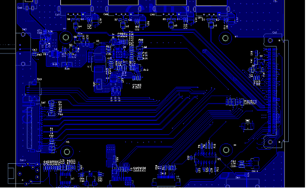
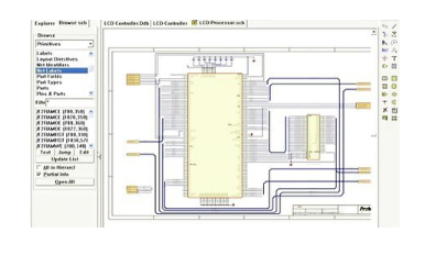
Computer Aided Design refers to the use of computers and their graphics devices to help designers design work.
In the design, a large number of calculations, analysis and comparisons of different schemes are usually carried out by computer to determine the optimal scheme; various design information, whether digital, text or graphic, can be stored in the memory or outside of the computer. Save and quickly retrieve; designers usually start with a sketch, and the heavy work of turning a sketch into a worksheet can be done by the computer; the design results automatically generated by the computer can quickly make the graph and make the designer timely The design makes judgments and modifications; the computer can perform graphic data processing related to editing, enlargement, reduction, translation, copying, and rotation of graphics.
As an outstanding engineering achievement, CAD technology has been widely used in various fields of engineering design. The development and application of CAD systems have caused profound changes in traditional product design methods and production models, resulting in huge social and economic benefits. At present, CAD technology research hotspots include computer-aided conceptual design, computer-supported collaborative design, massive information storage, management and retrieval, design method research and related issues, and support for innovative design. It is foreseeable that technology will have a new leap and will also cause a design change.

CAD technology has been continuously developed and explored. The application of CAD technology has played a role in improving the design efficiency of enterprises, optimizing design schemes, reducing the labor intensity of technicians, shortening design cycles, and strengthening design standardization. More and more people realize that CAD is a huge productivity. CAD technology has been widely used in machinery, electronics, aerospace, chemical, construction and other industries. Design methods such as parallel design, collaborative design, intelligent design, virtual design, agile design, and full life cycle design represent the development direction of modern product design patterns. With the further development of artificial intelligence, multimedia, virtual reality, information and other technologies, CAD technology is bound to develop in the direction of integration, intelligence and synergy. Enterprise CAD and CIMS technology must take a step-by-step approach with e-commerce as the goal. From the inside of the enterprise, realize integrated, intelligent and networked management, use e-commerce to cross the boundaries of the enterprise, and realize the agile supply chain between the customer, the enterprise and the supplier in the true sense.
Protel and cad differenceThe Protel series software is specially designed for circuit design. It can be used for circuit schematic drawing, PCB drawing and simulation analysis. It is more professional and CAD can do it, but it is not as professional as Protel in circuit design.
Protel99 is a professional circuit design software, which is more convenient and practical for circuit design!
Protel99 is to draw PCB board circuit, CAD is architectural, mechanical drawing, they can be exchanged by DXF format
CAD is mainly powerful in construction/mechanical drawing, in addition to designing a lot of things to draw and play a wide range of functions.
CAD is a very large drawing software that is widely used in the design field. It can draw construction drawing renderings and software that can be applied in various fields. Such as architectural design, interior design, product design, mechanical design, mechanical and electrical design, clothing design and so on!

1. The role of SCHMEDIT is mainly to get a beautiful circuit diagram
Wrong. The purpose of SCHMEDIT drawing is mainly to get a network table to prepare for the next printed board design. In fact, it is difficult to get a beautiful and nationally-compliant circuit diagram with Western SCHMEDIT.
2. To use TRAXEDIT for automatic routing, you must first draw a circuit diagram with SCHMEDIT.
Wrong. TRAXEDIT auto-routing does not require schematic support, nor is it not possible to draw with SCHMEDIT. TRAXEDIT just needs a network table (.NET) file. The network table can be drawn into a schematic diagram by SCHMEDIT, and then processed by POST.EXE. It can also be generated by other software (such as ORCAD) software. After understanding the network table, you can also manually prepare the network table file.
3. When wiring in TRAXEDIT, it must be 'regularly' wired according to the wiring method provided by it, otherwise a complete printed board diagram cannot be obtained.
wrong. In fact, as long as you draw a line on PROTEL's BOTTOM LAYER or TOP LAYER, or put a solder joint, this line or this solder joint can be made to the board, no matter how the line is drawn, or this How to do the solder joints, either using PROTEL's automatic line drawing or any line drawn with the F3 line drawing function. The solder joint can be on a component or a solder joint placed with the PLACE function. This may seem simple, but if you understand this, you can start working right away.
4. Single panel is simpler than double panel
wrong. It is much more difficult to make a single panel in PROTEL than a dual panel, and the routing rate is very low when using the automatic routing function.
5. The line that is wired with PROTEL is definitely correct.
wrong. The automatic wiring with PROTEL does not guarantee the correct wiring. Sometimes it will make a 'serious' error, such as a short circuit in the power supply. It must be thoroughly checked after the wiring is completed and carefully revised.
6. It is reasonable to use the PROTEL automatic routing function to lay out the line.
wrong. The line of the utility PROTEL automatic routing function is very messy, and it is not comparable to the manual wiring of experienced people, especially the wiring of analog circuits, which must be manually modified. Even full manual wiring can meet the requirements.
7. The package library of components in PROTEL is very comprehensive, generally do not need to increase the package library.
Wrong. The package of components in PROTEL is indeed a lot, but it is a little less than the package of many components we use. Sometimes an Electrolytic capacitor can not find a ready-made package. Therefore, using PROTEL to design the printed board, it is common to add a package library. It is very convenient to add a package library in PROTEL. It should be noted here that the package can not only look at the similar shape, so the name of the pad and the pin name of the component in the schematic are the same, otherwise the pin will be lost when the network table is transferred. (The pin name of the component can be transferred to the component using SLM to view it.) In this regard, some newspapers and magazines have been published recently, please refer to it.
8. After PROTEL has designed the printed board, it must be drawn with a plotter to go to the photo board.
wrong. A larger-scale printed board manufacturer can carry out a light-drawn version as long as you provide a painted picture. The effect is very good, and the cost is not high. Compare it. If a photo-made board is used, a double-sided plus solder resist is used. , the printed board, must provide 5 drawings (positive and reverse copper, positive and negative resistance welding and front silk screen), to take 8 negatives (positive and reverse copper and printing surface must first make negative, then remake positive ), and draw the board with light, as long as two pieces of film can be.

1. To implement PROTEL's automatic layout function, first have a network table (produced by the method described above), then enter TRAXEDIT, and set a wiring area in the prohibited wiring layer to use this function. The so-called wiring area is to draw a square in the prohibited wiring layer. The operation is as follows: After entering TRAXEDIT, use the '-' key to switch the layer. After seeing the bottom state line is KEEP OUT LAYER, press the F3 line drawing function to draw a box. The frame can be drawn at the beginning. Some, this has little effect on future wiring.
2. The method of drawing lines in TRAXEDIT. There are four wiring methods in ROTLE in the NETLIST function table, which are (1) BOARD, which is the wiring of the entire circuit board. (2) CONNECTION is the area line wiring, the method is to use the SHOW function in the NETLIST, display the flying line, then enter the ROTLE function, select CONNECTION, at this time, you can use the cursor to click the next flying line, you can use this flying line Automatic line. (3) MANUAL manual wiring, the method is to first display the flying line, then select a solder joint with a flying line, click with the mouse, you can use the mouse to drag the line, you can switch the layer during the line drawing. The above three line drawing functions must be transferred to the network table before they can be used. (4) PAD TO PAD is the pad to the pad. After selecting this item, first use the cursor to point one of the pads (either a single pad placed with the PLACE function or one of the pads). And then click on the other one, the program can automatically route the two pads. (5) F3 line drawing function, as long as you press F3, you can draw a line, this is the real hand-drawn line.
Semiconductor Fuse and Ferrite
Fuse refers to an electric appliance that, when the current exceeds the specified value, melts the fuse and disconnects the circuit with the heat generated by itself.When the current exceeds the specified value for a period of time, the fuse melts and disconnects the circuit with the heat generated by the fuse itself.A current protector made from this principle.The fuse is widely used in high and low voltage power distribution system and control system as well as power equipment.
Ferrite is a metal oxide with ferrous magnetism.As far as electrical properties are concerned, the resistivity of ferrite is much larger than that of single metal or alloy magnetic materials, and it has higher dielectric properties.Ferrite magnetic energy also shows high permeability at high frequencies.As a result, ferrite has become a non-metallic magnetic material widely used in the field of high frequency and weak current.Due to the low ferrite magnetic energy stored in the unit volume, saturated magnetic induction strength (Bs) and low (usually only pure iron 1/3 ~ 1/5), and thus limits its higher requirements in the low-frequency magnetic energy density in the field of high voltage and high power applications.
Semiconductor Fuse, Fuse Cutout, Protection Fuse, Square Fuse, Fuse Link, Ceramic Fuse, Fuse Box, Fuse Resistors
YANGZHOU POSITIONING TECH CO., LTD , https://www.yzpstcc.com