Principle and application of LM567 and NE567
Audio decoder 567 function overview This article discusses the phase-locked loop circuit and introduces the NE567 single-chip audio decoder integrated circuit. This tone decoding block contains a stable phase-locked loop and a transistor switch. When the predetermined audio is added to the input of this integrated block, a local wave can be generated. This audio decoder can decode tones of various frequencies. For example, to detect the touch tone of the phone. This audio decoder can also be used in BB machines, frequency monitors and controllers, precision oscillators and telemetry decoders.
This article mainly discusses Philip's NE567 audio decoder / phase-locked loop. This device is an inexpensive 567-type product in an 8-pin DIP package. Figure 1 shows the pin diagram of this package. Figure 2 shows the internal block diagram of this device. It can be seen that the basic components of NE567 are a phase-locked loop, a right-angle phase detector (quadrature phase detector), an amplifier, and an output transistor. The phase locked loop contains a current controlled oscillator (CC0), a phase detector and a feedback filter.
Philip's NE567 has a certain temperature operating range, namely 0 to + 70 ° F. The electrical characteristics are about the same as Philip's SE567, except that the SE567 has an operating temperature of -55 to 125 ° F. However, 567 has been designated as the industry standard audio decoder, and several other multi-national semiconductor integrated circuit manufacturers simultaneously produce this integrated block.
For example, Anal · g Device provides three kinds of AD567, EXar provides five kinds of XR567, and NaTIonal Sevniconductor provides three kinds of LM567. These 567 devices of different brands can work normally in the circuits discussed in this article. Therefore, this article refers to these devices as the 567 audio decoder.

The basic working condition of the 567 is like a low-voltage power switch. When it receives an input tone in the selected narrow frequency band, the switch is turned on. In other words, 567 can be a precise tone control switch.
The universal 567 can also be used as a variable waveform generator or a universal phase-locked loop circuit. When it is used as a tone control switch, the detected center frequency can be set to any value within 0.1 to 500KHz, and the detection bandwidth can be set to any value within 14% of the center frequency. Moreover, the output switching delay can be changed within a wide time range by selecting external resistance and capacitance.
The current-controlled 567 oscillator can change its oscillation frequency in a wide frequency band through an external resistor R1 and capacitor C1, but the signal through pin 2 can only be in a very narrow frequency band (the maximum range is about 14 of the free oscillation frequency %) Change its oscillation frequency. Therefore, the 567 phase-locked circuit can only "lock" in the very narrow frequency band of the preset input frequency value. The integrated phase detector of 567 compares the relative frequency and phase of the input signal and the oscillator output. Only when the two signals are the same (that is, the PLL lock) will produce a stable output. The center frequency of the 567 tone switch is equal to its free oscillation frequency, and its bandwidth is equal to the lock range of the PLL.
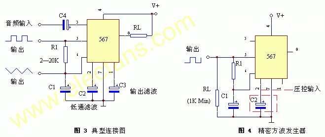
Figure 3 shows the basic wiring diagram when the 567 is used as a tone switch. The input tone signal is AC coupled to pin 3 through capacitor C4, where the input impedance is about 20KΩ. The external output load resistance RL inserted between the positive power supply terminal of the power supply and pin 8 is related to the power supply voltage. The maximum value of the power supply voltage is 15V, and pin 8 can absorb a load current of up to 100 mA.
Pin 7 is usually grounded, and pin 4 is connected to a positive power supply, but its voltage value must be a minimum of 4.75V and a maximum of 9V. If you pay attention to throttling, pin 8 can also be connected to the positive power supply of pin 4.
The center frequency (f0) of the oscillator is also determined by the following formula:
f0 = 1.1 × (R1 × C1) ············ (1)
Here the unit of resistance is KΩ, the unit of capacitance is uF, and the unit of f0 is KHz.
The equation (1) is shifted accordingly to obtain the value of the capacitor C1:
C1 ï¼ 1.1 / (f0 × R1) ············· (2)
Using these two formulas, the values ​​of capacitance and resistance can be determined, and the value of resistor R1 should be in the range of 2 to 20KΩ. Then, the capacitance value is determined by (2).
This oscillator generates an exponential sawtooth wave on pin 6 and a square wave on pin 5. The bandwidth of this tone switch (and the lock range of the PLL) is determined by a 3.9KΩ resistor inside C2 and 567. The output switching delay of this circuit is determined by C3 and a resistor in the integrated circuit.
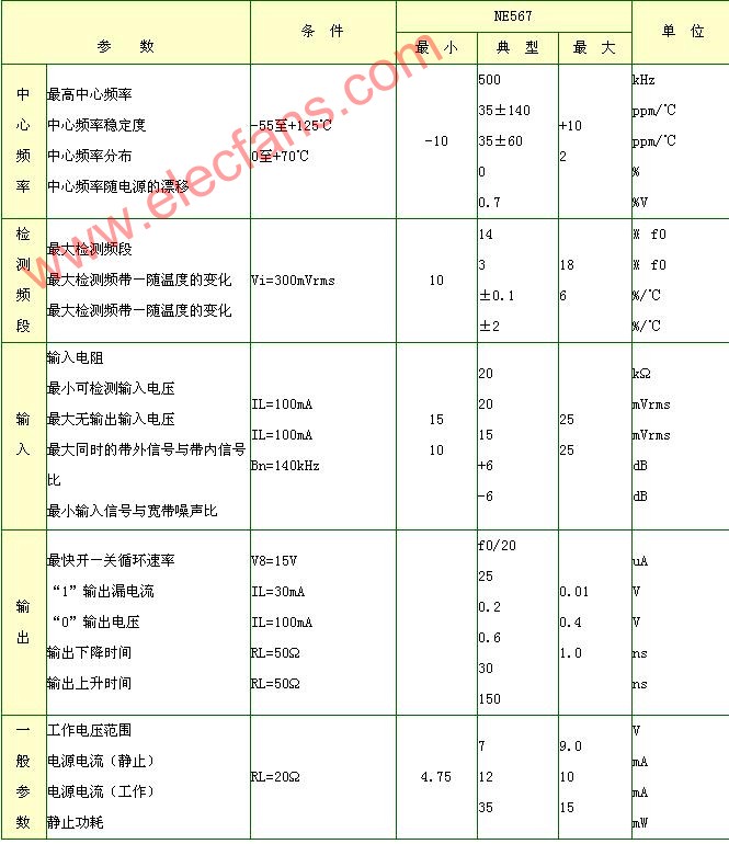
Table 1 lists the electrical characteristics of Philip's NE567. All other manufacturers' 567 chips with different brands have the same characteristics as Table 1.
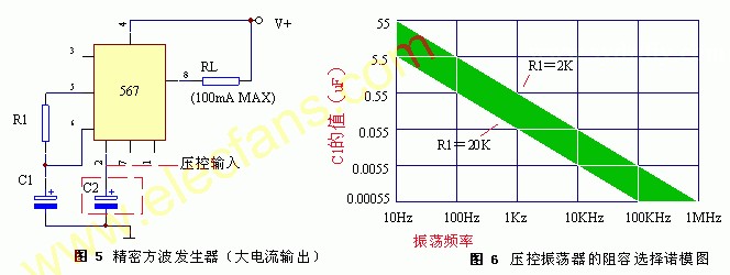
Figures 4 and 5 show how to make the 567 produce a precise square wave output. A non-linear sawtooth wave can be obtained from pin 6, but its use is limited, however, a square wave with excellent performance can be obtained on pin 5. As shown in Figure 4, the rise time and fall time of the output square wave is 20nS.
The peak-to-peak amplitude of this square wave is equal to the power supply voltage minus 1.4V. This square wave generator and load characteristics are excellent, any resistive load greater than 1KΩ will not affect the function of the circuit. In addition, the output of this square wave generator can also be added to a low impedance load. As shown in Figure 5, the peak current at the output of pin 8 is up to 100mA, but the waveform is slightly worse.
Using the aforementioned oscillation frequency and capacitance calculation formulas (1) and (2), various parameters of this type of oscillator can be determined. Similarly, R1 must be limited to the range of 2 to 20KΩ. In order to simplify the calculation and save time, the value of the component that determines the oscillation frequency can also be directly read from the nomogram shown in FIG. 6.
For example, if the 567 oscillator needs to work at 10KHz, the values ​​of C1 and R1 can be 0.055uF and 2KΩ, or 0.0055uF and 20KΩ.
Adding a control voltage to pin 2 of 567 can fine-tune the operating frequency of the oscillator within a narrow range by a few percent. If the control voltage is added, pin 2 should be connected to decoupling capacitor C2, and its value should be roughly twice that of C1.
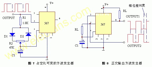
The circuits of FIGS. 4 and 5 can be modified in different ways, as shown in FIGS. 7 to 10. In FIG. 7, the duty cycle or the mark / space ratio is completely variable with respect to the generated waveform. With the help of the trimming potentiometer R2, the variation range is 27: 1 to 1:27. In addition, in each working cycle, C1 alternately charges and discharges, the charge is through the left side of resistors R1, diodes D1 and R2, and the discharge is through the right side of resistors R1, diodes D2 and R2. Only with the change of the mark / space ratio, the working frequency changes slightly.
The circuit shown in Figure 8 can generate a quadrature square wave. The two square wave outputs on pins 5 and 8 of this oscillator have a 90 ° phase difference. In this circuit, input pin 3 is connected to ground. If a bias voltage of more than 2.8V is added to pin 3, the square wave on pin 8 has a 180 ° phase shift.
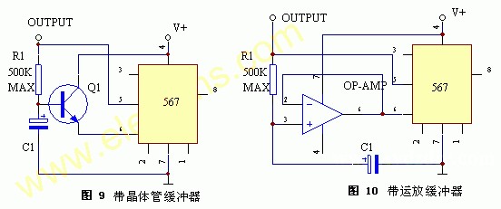
Fig. 9 and Fig. 10 show the circuit of the oscillator whose timing resistance value can be up to about 500KΩ. In this way, the value of the timing capacitor C1 can be reduced proportionally. In these two circuits, there is a buffer stage indirectly between the pin 6 of 567 and the nodes of R1 and C1.
In Figure 9, this buffer stage is a first-stage transistor-emitter follower. Unfortunately, the introduction of this stage makes the waveform symmetry slightly worse. Correspondingly, the circuit shown in Figure 10 uses a first-stage operational amplifier follower as a buffer stage. This does not affect the symmetry of the waveform.
Five outputs of 567 Five output terminals of 567. Two of them (pins 5 and 6) provide the output waveform of the oscillator, and the third output terminal pin 8 is the main output port of 567 as mentioned above. The remaining two outputs are pins 1 and 2 of the decoder.
Pin 2 is connected to the output of the phase detector of the phase-locked loop, and is internally statically biased to 3.8V. When the 567 receives the in-band input signal, the bias voltage changes accordingly, and in the typical 0.95 to 1.05 times the oscillator free oscillation frequency range, the change in the bias voltage is linear with the input signal frequency. The slope is 20mV per frequency deviation (ie 20mV / f0).
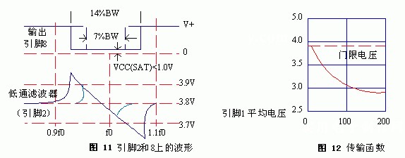
Figure 11 shows the time relationship between pin 2 output and pin 8 output when 567 is used as a tone switch. The figure shows the time relationship between the two bandwidths (14% and 7%).
Pin 1 gives the output of 567 quadrature phase detection. When the tone is locked, the average voltage on pin 1 is a function of the amplitude of the input signal in this circuit, as shown in the transfer function in Figure 12. When the average voltage on pin 1 is pulled below the 3.8V threshold, the internal output transistor of the collector on pin 8 turns on.
Determination of bandwidth When 567 is used as a tone switch, the maximum value of its bandwidth (percentage of center frequency) is about 14%. This value is proportional to the in-band signal voltage of 25 to 250mV rms. However, when the signal voltage changes from 200 to 300mV, it does not affect the bandwidth. At the same time, the bandwidth is inversely proportional to the product of the center frequency f0 and the capacitor C2. The actual bandwidth is:
BW ï¼ 1070
The unit of BW is the percentage (%) of the center frequency, and Vi≤200mVRMS. In the formula, the unit of Vi is V-RMS, and the unit of C2 is uF.
C2 is selected through trial and error processing. At the beginning, the value of C2 can be selected to be twice that of C1. Subsequently, the value of C2 can be increased to reduce the bandwidth, or the value of C2 can be decreased to increase the bandwidth.
Symmetry of the detection bandwidth The so-called detection of the symmetry of the facelift is to measure the degree of symmetry between this bandwidth and the center frequency. The definition of symmetry is as follows:
(Fmax + fminï¼2f0) / 2f
At this time, fmax and fmin are the frequencies corresponding to the two edges of the detected frequency band.
If the center frequency of a tone switch is 100KHz and the bandwidth is 10KHz, the edge frequency of the frequency band is symmetrical to 95KHz and 105KHz, so that its symmetry is 0%. However, if the frequency band is quite asymmetric, the edge frequencies are 100KHz and 110KHz, and the symmetry value increases to 5%.
If necessary, you can use trimmer potentiometer R2 and 47KΩ resistor R4 to add an external bias trimmer voltage on pin 2 of 567 to reduce the symmetric value to 0, as shown in Figure 13. Move the middle sliding contact of the potentiometer upward to decrease the center frequency, and move downward to increase the center frequency. Silicon diodes D1 and D2 are used for temperature compensation.
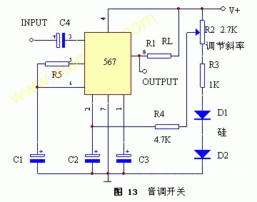
Based on the typical circuit shown in Figure 13, it is easy to design a practical tone switch. The nomogram of FIG. 6 can be used to select the values ​​of the frequency control element resistance R1 and the capacitance C1. The selection of the capacitance C2 can be based on the above discussion and determined by experiment. At first, a capacitor with a capacity twice that of C1 can be used, and then, if necessary, the value can be adjusted to give the required signal bandwidth. If the requirements for the symmetry of the frequency band are strict, a symmetry adjustment stage can be added as shown in FIG. 13.
Finally, make the value of C3 twice that of C2. And check the response of this circuit. If C3 is too small, the output on pin 8 may pulse during the switching due to the transition history. If C3 is selected properly, the entire circuit is designed.
Any number of 567 tone switches can be fed from one audio input to form a multi-tone switch network of any desired size. Figures 14 and 15 are two practical two-level switching networks.
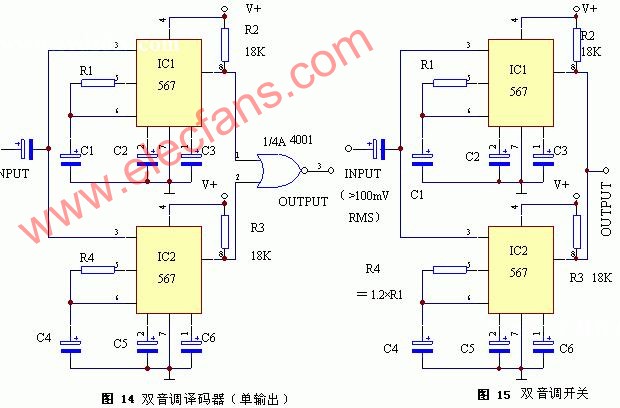
The circuit in Figure 14 functions as a dual tone decoder. When any of the two input and input signals appears, a signal output can be excited. In the figure, the two tone switches are excited by a signal source, and the output is NOR processed by a CD4001B type CMOS gate integrated block. Figure 15 shows that two 567 tone switches are connected in parallel, which has a single tone switch with a relative bandwidth of 24%. In this circuit, the operating frequency of the IC1 tone switch is designed to be 1.12 times higher than the operating frequency of the IC2 tone switch. Therefore, their switching bands are overlapping.
Wifi App Robot Vacuum Cleaners
Wifi App Robot Vacuum Cleaners,Intelligent Robot Vacuum Cleaner,Gyro Navigation,Smart Memory
NingBo CaiNiao Intelligent Technology Co., LTD , https://www.intelligentnewbot.com