RFID (Radio Frequency Identification) is a rapidly evolving automatic identification technology that has gained significant attention in recent years. It utilizes radio frequency signals for non-contact, two-way communication to enable data exchange and identification. As a key enabler of high-speed, real-time, and accurate information collection and processing, RFID holds great potential across various industries such as manufacturing, retail, logistics, and transportation. Globally, RFID is recognized as one of the most important technologies of the 21st century.
An RFID tag consists of an antenna and a chip, both of which have complex impedance characteristics. For passive tags, all power needed for operation is supplied by the reader through RF energy. The efficiency of power transfer between the antenna and the chip depends on their impedance matching, which directly impacts the overall performance of the system. Therefore, achieving good impedance matching is critical for reliable tag functionality.
Current impedance matching techniques are often complex and result in low recognition accuracy when applied to RFID chips, leading to unsatisfactory performance. To address this, this paper proposes a low-cost impedance matching network designed specifically for passive RFID tags. The network is integrated within the tag chip, featuring a simple structure that enables efficient power transmission between the antenna and the chip, as well as between the tag and the reader. This improvement enhances chip performance and increases the reader’s ability to accurately detect reflected signals from the tag.
**1. RFID Tag Impedance Matching Analysis**
**1.1.1 RFID Principle and Tag Composition**
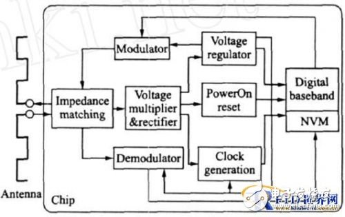
A typical RFID system comprises a reader and a tag. The reader sends a continuous wave (CW) signal to the tag, which activates the chip and modulates commands and data into radio frequency electromagnetic waves. The tag, located within the reader’s electromagnetic field, uses a voltage doubler rectifier circuit to increase the input voltage to the level required for normal chip operation, converting AC to DC. The output voltage is then stabilized using a voltage regulation circuit. The demodulation module extracts the command and data from the received CW signal, passing it to the digital baseband module, which processes the data according to the protocol. When returning data, the tag alters its antenna’s reflection coefficient by changing its impedance, sending a modulated signal back to the reader. A clock generation circuit provides the necessary clock frequency, and a power-on reset circuit ensures proper initialization of the baseband processor and modulation circuits.
Figure 1 shows the block diagram of the RFID tag system. The chip includes three main components: the RF analog front end, the digital baseband, and non-volatile memory (NVM). The analog front end handles functions like impedance matching, voltage doubling, modulation, demodulation, voltage regulation, power-on reset, and clock generation.
**1.1.2 Impedance Matching Analysis**
Figure 2 illustrates the Thevenin equivalent circuit of the RFID tag, widely used by researchers to analyze antenna performance. The open-circuit AC voltage induced on the antenna is denoted as Va, while Vc represents the chip's input voltage. The antenna input impedance is Za = Ra + jXa, and the chip input impedance is Zc = Rc + jXc. The real part of the chip's impedance is mainly determined by the voltage doubler and load, while the imaginary part is influenced by the rectifier, modulation/demodulation circuits, and ESD protection. Both Za and Zc vary with frequency, and Zc also changes with input power. In this study, the impedance matching network is designed for the minimum power required for chip operation. To achieve maximum power transfer, the chip’s input impedance must be conjugate-matched with the antenna.
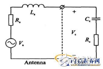
The L-type matching method is commonly used for efficient RF-to-DC conversion. However, integrating inductors in small areas is impractical for RFID chips. Instead, the chip’s input impedance is adjusted using inductance La to achieve L-type matching. When two devices with complex impedances are connected, the complex power wave reflection coefficient at the interface is defined as S. This concept applies to RFID tags:
$$ S = \frac{Z_c - Z_a}{Z_c + Z_a} $$
In the conjugate matching state (state 0), the chip’s input impedance is Zc0, while in the mismatched state (state 1), it is Zc1. Through impedance correction, the imaginary part of the antenna impedance is canceled, leaving only the real part Ra. The chip’s input voltage can then be calculated using the following equation:
$$ V_c = \frac{V_a \cdot R_a}{\sqrt{(R_a + R_c)^2 + (X_a - X_c)^2}} $$
Since the power for passive RFID chips comes entirely from the electromagnetic field, the input voltage Vc must be sufficiently high to activate the voltage doubler and provide stable operating voltage, making it a crucial parameter for tag performance.
The radar cross section (RCS) of the RFID tag is a function of the chip’s input impedance. Using the classical radar equation, the RCS value is calculated as:
$$ \text{RCS} = K^2 G^2 \left| \frac{Z_c - Z_a}{Z_c + Z_a} \right|^2 $$
Where K is the wavelength and G is the antenna gain. Different RCS values corresponding to different chip impedance states allow the reader to distinguish the tag’s transmitted data based on the amplitude of the reflected signal. The vector differential RCS further enables the reader to detect the phase characteristics of the modulated signal, represented as ΔV:
$$ \Delta V = \frac{Z_c - Z_a}{Z_c + Z_a} $$
**2. Proposed Impedance Matching Network**
**2.1.1 Principle Analysis**
When the tag operates in the 923 MHz band and the chip is under minimum input power, the Agilent E5071C network analyzer measures the chip’s input impedance as 22 - j106 Ω. A high-Q tag antenna with an input impedance of 15 + j88 Ω is selected. The impedance matching network design is shown in Figure 4, where La = 1512 nH.
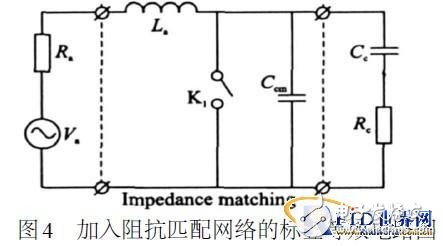
When switch K1 is open, the chip is in state 0. In the matching path from the chip’s input impedance to the antenna’s conjugate impedance (as shown in Figure 5), the impedance at point 1 is 22 - j106 Ω. After adding a parallel capacitor Ccm, the resistance at point 2 is approximately 158 Ω, and the impedance becomes 15 - j888 Ω. Adding a series inductance La brings the impedance to 158 Ω, achieving conjugate matching with the corrected antenna impedance. Calculations show that Ccm = 340 fF.

With no complex power wave reflection at the antenna-chip interface, conjugate matching allows the antenna to transfer half of the RF energy to the chip, maximizing power transfer. When switch K1 is closed, the chip enters state 1. Figure 6 shows the change in the chip’s input impedance.

**2.1.2 Performance Comparison**
Without impedance matching, the chip’s Qc is 4182. After adding the impedance matching network, Qc increases to 5187 under conjugate matching conditions, resulting in a 111-fold increase in the chip’s output voltage Vc, significantly improving its performance. The modulus of the vector differential RCS of the chip reaches 1015 dB, greatly enhancing the readability of the reflected signal and improving the accuracy of tag recognition by the reader.
**2.1.3 Circuit Implementation**
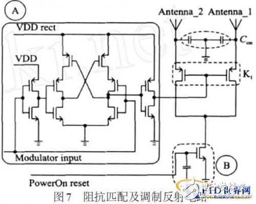
The impedance matching network consists of a capacitor Ccm and a switch K1, as shown in Figure 7. To ensure symmetry between the two antenna pins, Ccm is implemented as two parallel capacitors, each of 170 fF. K1 is composed of two PMOS switches driven by a level conversion circuit controlled by the baseband signal, ensuring the gate voltage is sufficient to reliably turn off the PMOS. Part B includes a power-on protection circuit, stabilizing the power-on reset signal before the digital baseband circuit initializes, preventing unintended reflections due to unstable chip states. Both the PMOS and NMOS transistors use a mesh gate structure to increase the width-to-length ratio, reducing resistance and parasitic capacitance.
**3. Test Results**
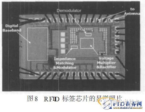
The designed RFID tag chip is fabricated using the charted0135Lm2P4M low-threshold CMOS process, with a chip size of 1026 μm × 1796 μm. Figure 8 shows a photomicrograph of the chip. In practice, only two pins are connected to the antenna, while the remaining pins are used for testing and connecting analog or digital signals.
The output level of the voltage doubler circuit is a key performance indicator. With an input AC level of just 300 mV, the chip’s DC output reaches 1.147 V, meeting the operational requirements. The RFID operating band specified in ISO18000-26C is 860–960 MHz, aligning with China’s 920–925 MHz regulation. Thus, the tag operates in the 923 MHz band.
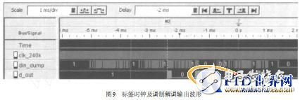
Using an Impinj Speedway reader with a transmit power of 2 WERP and a tag antenna gain of 11.5 dBi, the signal waveform was tested using an Agilent 1682A logic analyzer. Figure 9 shows the system clock “clk-240k†at 240 kHz, the demodulated output “din-dump,†and the modulated output “d-out.†The test results show that the tag using the impedance matching network achieves a bit error rate below 10â»â´, demonstrating improved accuracy in tag recognition.
**4. Conclusion**
This paper presents a low-cost impedance matching network for passive RFID tags compliant with the ISO18000-26C standard. The circuit is simple and effectively maximizes power transfer between the reader, tag antenna, and chip. The proposed method was verified using the charted0135Lm CMOS process. Both theoretical analysis and measured results confirm that the approach significantly improves chip performance and reader recognition accuracy, meeting the system design requirements.
ac dc adapter,dc adapter,ac adapter 12v,dc power adapter,ac dc adapter 24v
FOSHAN SHUNDE KELICHENG POWER SUPPLY TECHNOLOGY CO., LTD , https://www.kelicpower.com