The high-power wide-band linear RF amplifier module is widely utilized in critical communication systems such as electronic warfare, radar, and detection. Its broadband and high-power generation technology plays a vital role in modern wireless communication systems. As wireless communication technologies continue to evolve, the demand for broadband high-power amplifiers has increased, particularly with the development of wideband frequency hopping and spread spectrum techniques. This has led to a need for solid-state linear power amplifiers that can operate over a broader frequency range and deliver higher output power while maintaining good linearity and modularity.
In general, broadband RF power amplifiers designed for the HF to VHF bands typically employ FETs rather than traditional power transistors. This is due to the high input impedance of FETs, which allows for easier impedance matching and a simpler biasing circuit. Additionally, FET-based amplifiers offer higher gain and better linearity, making them ideal for high-performance applications.
This paper presents a high-power wide-band linear RF amplifier designed using MOSFETs. It operates in class AB push-pull mode, covering a frequency range from 6 MHz to 10 MHz with an output pulse power of 1200 W. After thorough testing and adjustment, the amplifier demonstrates stable performance and reliability. The testing process involved various instruments, including a signal generator, spectrum analyzer, power meter, high-power coaxial attenuator, network analyzer, and a multiplier.
**1. Pulse Power Amplifier Design**
**1.1 Circuit Design**
The designed broadband high-power pulse amplifier module requires a working frequency band exceeding four octaves and must provide significant output power with strong harmonic suppression. Since harmonics may fall within the operating frequency range, the design must ensure a high level of linearity. To meet these requirements, the RF power amplifier uses a three-stage FET configuration, all based on MOSFETs. Each stage operates in class AB mode and employs a push-pull structure to ensure broad bandwidth operation.
To simplify the power supply design, an enhancement-mode MOSFET is used. Transmission line broadband matching and feedback circuits are incorporated to enhance performance across the entire frequency range. Due to the requirement for high-power pulsed emission, the first and second stages use MOSFETs (IRF510 and IRF530) capable of fast switching to preserve the integrity of the pulse modulation signal and reduce interference. For the final stage, which needs to deliver 1200 W of output power, the MOSFET MRFl57 is selected without the need for power synthesis techniques.
The schematic of the designed RF pulse power amplifier is shown in Figure 1.
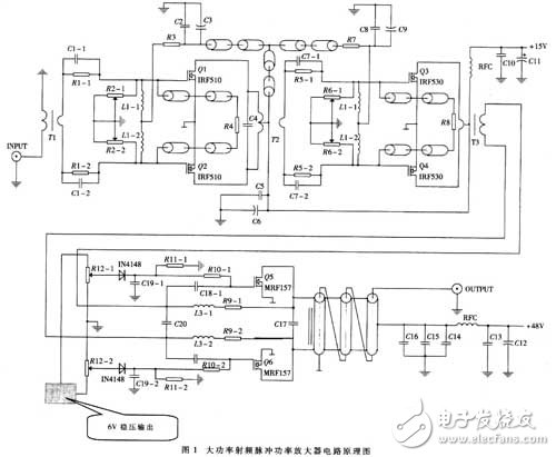
The signal path begins at the source, passes through intermediate amplification stages, and is then amplified by the power stage before being transmitted via the antenna. In the schematic, the input signal is 20–21 dBm at 50 Ω, with a working voltage of 15 V and 48 V. The 15 V powers the first two stages, while the 48 V supplies the final stage. A 6 V regulated output can be derived from either voltage source. The overall design uses class AB amplification, with a standing wave ratio of 1.9.
After intermediate amplification, the signal undergoes impedance transformation via T1 (4:1), then enters the power amplifier. The upper half of the signal turns on Q1, and the lower half turns on Q2. The signal then goes through T2 (16:1) for further amplification. Q3 and Q4 handle the upper and lower halves of the signal, respectively, ensuring full-cycle energy amplification. Impedance transformation via T3 (4:1) prepares the signal for the final stage, where the current is increased to drive the high-power MOSFET MRFl57. Finally, T4 (1:9) ensures a 50 Ω output impedance match.
Negative feedback is implemented in the circuit to maintain stable power gain across the entire frequency band, improve linearity, and enhance input return loss stability, especially at low frequencies.
Each stage also includes a varistor to set the bias voltage of the transistors, reducing crossover distortion and ensuring a clean waveform in both the upper and lower signal cycles.
**1.2 PCB and Transmission Line Transformer Design**
To ensure consistent signal amplification across the entire frequency range and minimize clutter and harmonics, the design emphasizes symmetry in the class AB power amplifier. During PCB layout, care is taken to make copper traces symmetrical and of equal length. A lead-tin light board is used to facilitate dielectric constant selection, and Smith chart software is employed to simulate and optimize copper trace shapes for optimal impedance matching.
A key aspect of the design is the fabrication of transmission line transformers, which enable impedance matching between the signal source and the power MOSFETs. These transformers maximize the tube’s bandwidth potential. Two important design considerations include the impedance relationship between the source, load, and transmission line, as well as proper connection and grounding methods. Due to the class AB configuration, the primary and secondary coils should be as symmetrical as possible.
Four transmission line transformers (T1, T2, T3, and T4) are used in the design. T1 and T2 have one turn on their secondary coils, while T3 has two turns to prevent magnetic saturation at low frequencies. T1, T2, and T3 use the SFF-1.5-1 coaxial core for the primary coil, with copper foil for the secondary. T4 is an imported high-power transformer (model: RF2067-3R).
**1.3 Thermal Design**
Due to the high power consumption and heat generation in RF power amplifiers, effective thermal management is essential. Based on the power dissipation of each stage and the thermal characteristics of the components, the required heat sink size and material are determined. In this design, the operating temperature is 55°C, and an aluminum heat sink measuring 290 mm × 110 mm × 35 mm is used. A DC fan is also required to cool the final MOSFET (MRFl57).
**2. Assembly and Commissioning of the Pulse Power Amplifier**
All amplifier tubes in the design are MOSFETs, which are highly sensitive to static electricity. Special care is taken during soldering, especially when handling the high-power MOSFET (MRFl57). Before circuit design, it is recommended to simulate the behavior of IRF510 and IRF530 using software like Multisim or PSpice.
During initial debugging, the bias voltage of the last stage MOSFET (MRFl57) can be temporarily omitted. Instead, the static operating point is set using the amplification effect of the first two stages. The output from the first two stages is approximately 100 Vpp (high impedance input). The operating point voltage should be slightly above the threshold voltage, and the power supply current must be monitored to avoid excessive current flow.
Fine adjustments to the gate-end transformer help minimize waveform distortion. An oscilloscope is used to monitor the output waveform. The first stage mainly affects the amplitude, while the second stage influences the waveform shape.
When debugging the final stage, extra caution is required due to the high cost of MRFl57. The static working voltage should be set carefully, and the static operating point should not be changed dynamically. The output is connected to a spectrum analyzer through a 5011 high-power coaxial attenuator to measure output power and harmonic content.
The wideband high-power amplifier was assembled and tested in a laboratory environment. Long-term testing with a transmitting coil confirmed its reliable operation. The amplifier meets the design specifications and performs well in practical applications, demonstrating its effectiveness in detection systems operating within the specified frequency range.
Vapme Shisha Hookah Vapes,Best Price VAPME Shisha Disposable Vapes, 15K PUFF Shisha Hookah Vape, Rechargeable Vapes VAPME Shisha, Vapme shisha Vape Pens
Shenzhen Essenvape Technology Co., Ltd. , https://www.essenvape.com