Graphene as a substrate for electronic products has attracted the attention of many large companies, such as IBM and Samsung, mainly due to its electron mobility - theoretically up to 200000 cm2/Vs, while silicon is only 1400 cm2/Vs, and indium antimonide has 77000 cm2/ Vs, this means ultra-high-speed electron migration. However, this figure is only theoretical. In reality, we still have a long way to go. But this will probably increase the speed of electronic equipment by nearly 1,000 times. This is a jump from Gigabit to terahertz. No wonder people are looking forward to this.
Graphene's 'Achilles' heel'
In the 'Graphene Roadmap' (a paper co-authored by researchers from the Nobel Prize winner at the University of Manchester and researchers from Texas Instruments, Samsung and other institutes) there is a warning about this optimism:
'Because graphene has no bandgap, there is little hope of using graphene as a high-performance integrated logic circuit in the next decade. '
In other words, its on/off ratio is not good. The on/off ratio refers to the difference between the electrical conductivity when the device is turned on and off. If the ratio is too low, the transistor will still conduct electrons even if it is already turned off. A device with a large number of transistors will therefore lose a great deal of energy and thus only become a heater. This limits the use of graphene in devices with logic cells.
However, because of its potential benefits after microelectronics success, the bandgap problem has not prevented the world's large electronics companies from developing graphene-based electronic devices. Samsung and IBM are very active in this field.
IBMvsSamsung
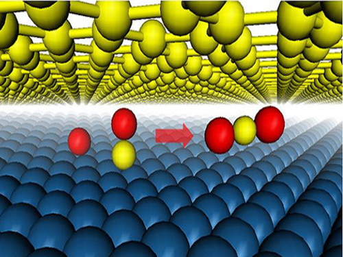
IBM claims that it has built the world's most advanced graphene-based chip, which is nearly 10,000 times more excellent than other graphene sheets - indicating that previous attempts were not perfect. From the CMOS manufacturing point of view, graphene is not an excellent material. It is quite fragile, so when you deposit and etch other materials at near atomic layer thickness, graphene is easily damaged. Therefore, although it is possible to fabricate the graphene channel of a transistor by depositing graphene, all subsequent processing steps may damage it, ultimately rendering it without advantages.
IBM's breakthrough idea is the final deposition of graphene. Compared to in-situ deposition, they tend to grow graphene on copper foil by chemical vapor deposition, and then dissolve the copper foil, leaving behind a layer of graphene that can be 'scrubbed' by the chip. This seems to be difficult to correlate with the manufacturing processes that are commonly used in the semiconductor industry, and it has been reported that the quality of the graphene thus prepared is poor, and the way of disposal of the copper foil is rather wasteful and expensive.
The different approach Samsung has adopted, namely the growth of high-quality monocrystalline graphite technology on silicon chips, is known as one of the most significant breakthroughs in the history of graphene research. Like IBM's method, this technology produces graphene sheets that can be used in microelectronics. Due to the high resistance, making a viable device seems far-fetched, but now Samsung seems to be more concerned about the flexibility of the device and the screen.
In addition to transistors, the high conductivity of graphene to electrons can be more widely used in other integrated circuits, such as conductors, to make CMOS circuits cheaper and more efficient.
HVAC Spare Parts including all spare parts of HVAC products, covering products of Air Conditioner, heat pumps, dehumdifiers, heater., etc.
Hvac Spare Parts,Air Conditioner Pipe Cover,Air Conditioner Compressor,Heavy Duty Outdoor Unit Bracket
Foshan Dinghan Electrical Technology Co., Ltd , https://www.dinghanelectrical.com