1. Using a pointer-type multimeter to judge the FET
(1) Using the resistance method to identify the electrodes of a junction field-effect transistor (JFET). The JFET has a PN junction, and the forward and reverse resistance values differ. By measuring the resistance between any two electrodes, you can determine which ones are the drain (D) and source (S), as they typically have similar resistance values (in the range of several thousand ohms). The remaining electrode is the gate (G). You can also use the black meter lead to touch one electrode and measure the resistance with the red lead on the other two. If both readings are approximately equal, the electrode touched by the black lead is the gate.
If the measured resistance is high, it indicates an N-channel FET, and the black lead is connected to the gate. Conversely, if the resistance is low, it's a P-channel FET. If no clear pattern emerges, swap the leads until the gate is identified.
(2) Determining the quality of the FET using the resistance method
To assess the condition of the FET, measure the resistance between the source and drain (R_DS), gate and source (R_GS), and gate and drain (R_GD). A good FET should show high resistance between the gate and the other terminals, while the source-drain resistance should be in the tens to thousands of ohms. If the resistance is too high or infinite, the FET may be faulty. Use the R×10k setting for more accurate measurements.
(3) Estimating the amplification capability of the FET using an inductive signal input method
Set the multimeter to R×100, connect the red lead to the source and the black lead to the drain. Then, pinch the gate with your hand to apply an induced voltage. This should cause a noticeable swing in the meter needle due to the FET’s amplification effect. A large swing indicates good amplification; a small or no swing suggests a weak or faulty FET.
This method works for both JFETs and MOSFETs, though for MOSFETs, avoid touching the gate directly with your hands. Instead, use an insulated tool to prevent damage from static electricity.
(4) Identifying unmarked FETs using the resistance method
By measuring resistance between pairs of pins, you can identify the drain and source. The remaining pins are the gates. After identifying D and S, verify the results using the amplification test. Once the positions of D, S, G1, and G2 are determined, the FET can be correctly installed in the circuit.
(5) Judging transconductance by measuring reverse resistance changes
For VMOS N-channel enhancement FETs, connect the red lead to the source and the black lead to the drain. When the gate is touched, the reverse resistance should change significantly. A larger change indicates higher transconductance.
Second, usage tips for FETs:
(1) Always stay within the maximum ratings for power dissipation, drain-source voltage, gate-source voltage, and current when designing circuits.
(2) Ensure correct biasing and polarity. For example, the gate of an N-channel FET must not be positively biased, and the gate of a P-channel FET must not be negatively biased.
(3) Due to their high input impedance, MOSFETs must be stored with their pins shorted. Use metal packaging to protect against external electrical interference. Avoid storing them in plastic boxes.
(4) To prevent gate breakdown, ensure all tools, workstations, and soldering irons are properly grounded. Short the source and drain before soldering, and remove the short after. Never plug or unplug FETs while the power is on.
(5) When installing FETs, avoid placing them near heat sources. Secure the package to prevent vibration. Bend the pins carefully to avoid damage.
For power FETs, proper heat sinking is essential. High current operation requires a well-designed heatsink to keep the device temperature within safe limits.
In summary, using FETs safely involves many precautions. Whether you're a professional or an electronics enthusiast, following these guidelines ensures reliable performance and longevity.
Three. VMOS FET
The VMOS FET (VMOSFET) is a high-efficiency power switching device developed after the standard MOSFET. It combines the advantages of high input impedance, low drive current, high voltage tolerance, and large operating current. It is widely used in amplifiers, power supplies, and inverters.
VMOS FETs have extremely high input impedance and a large linear amplification area. They also feature a negative current temperature coefficient, meaning that the on-current increases with temperature, preventing secondary breakdown. This makes parallel connections common.
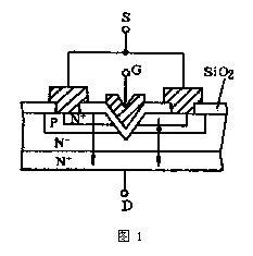
Unlike conventional MOSFETs, VMOS FETs have a V-groove gate and vertical current flow. The drain is located on the back side of the chip, allowing for higher current capacity and improved thermal management.
Major manufacturers include 877 Factory, Tianjin Semiconductor Device 4, and Hangzhou Electronic Tube Factory. Common models include VN401, VN672, and VMPT2.
Detection methods for VMOS FETs:
1. Identify the gate (G): Set the multimeter to R×1k. If a pin shows infinite resistance to the other two, it is the gate.
2. Determine source (S) and drain (D): Measure the resistance between the two remaining pins. The lower resistance value corresponds to the forward resistance, with the black lead connected to the source and the red lead to the drain.
3. Measure the on-state resistance (RDS(on)): Short the gate and source, then set the multimeter to R×1. The resistance should be in the range of a few ohms to ten ohms.
4. Check transconductance: Set the multimeter to R×1k or R×100, connect the red lead to the source and the black lead to the drain. Touch the gate with a screwdriver. A noticeable deflection of the needle indicates good transconductance.
Precautions:
(1) Most VMOS FETs are N-channel. For P-channel types, swap the test leads during measurement.
(2) Some VMOS FETs have protection diodes between the gate and source, making certain tests invalid.
(3) Power modules like IRFT001 are available for motor control and inverters.
(4) UHF power FETs such as the VNF series are suitable for high-speed switching and communication systems.
(5) Proper heat sinking is essential for high-power VMOS FETs. For example, the VNF306 can reach 30W with a suitable heatsink.
(6) When multiple FETs are used in parallel, parasitic oscillations may occur. Limit the number to four and add anti-oscillation resistors to each gate.
Features
â—† Small Compact Size,Global safety approvals
â—† Long life & high reliability.
â—† Wide Range of wires Terminals.
â—†Variety of actuator and terminals
â—†Customized Designs
â—†Widely used in household appliances, electric force, telecommunications, machine tool, vessel, textile, printing, Mining machine, Mustic Instrument, etc.
Miniature Micro Switch,Ultra Miniature Micro Switch,Micro Miniature Slide Switch,Miniature Snap Action Switch
Ningbo Jialin Electronics Co.,Ltd , https://www.donghai-switch.com