Connection/reference device
AD7176-2 24-bit, 250 kSPS Σ-Δ ADC with setup time 20 μs
AD8475 Precision, Selectable Gain, Fully Differential Funnel Amplifier
ADR445 5 V Ultra Low Noise LDO XFET Voltage Reference
Evaluation and design support
Circuit evaluation board
AD7176-2 Circuit Evaluation Board (EVAL-AD7176-2SDZ)
System Demonstration Platform (EVAL-SDP-CB1Z)
Design and integration files
Schematic, layout file, bill of materials
Circuit function and advantage
When sampling industrial level signals, fast high resolution conversion information must be provided. Typically, analog-to-digital converters (ADCs) have a maximum resolution of 14 bits to 18 bits when the sampling rate reaches 500 kSPS. The circuit shown in Figure 1 is a single-supply system optimized for industrial-level signal sampling, integrating a 24-bit, 250 kSPS Σ-Δ ADC. Each of the two differential channels or four pseudo differential channels can It is scanned at 17.2 bits of noise-free code resolution at a rate of up to 50 kSPS.
This circuit uses an innovative differential amplifier with built-in laser trimming resistors to perform attenuation and level shifting, and a precision ADC with low supply voltage can be used to achieve standard industrial-level signals of ±5 V, ±10 V, and 0 V to 10 V. The problem of digitizing. Applications for this circuit include process control (PLC/DCS modules), medical and scientific multichannel instruments and chromatographs.
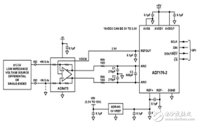
Figure 1. High-precision, 24-bit ADC driver for industrial signals (schematic diagram: all connections and decoupling not shown)
Circuit description
Industrial level signals are applied to the AD8475 precision differential funnel amplifier, which attenuates the input signal by a factor of 0.8 or 0.4. It integrates precision-adjusted and matched resistors to control attenuation. When the AD8475 uses a single 5 V supply and the gain is set to 0.4, this resistor supports single-ended or differential inputs up to ±12.5 V. The device provides input overvoltage protection up to ±15 V.
When the input signal (gain 0.4) is within ±10 V single-ended or differential input range, the AD8475 and AD7176-2 device combinations maintain linearity, as shown by the measured INL limit in Figure 4; Are they? 10 V and +10 V. At this point, the output swing of the AD8475 is between 0.5 V and 4.5 V.
The common mode output can be set by applying the desired common mode voltage to the VOCM pin. In the circuit shown in Figure 1, the common-mode voltage is set by applying the 2.5 V REFOUT voltage of the AD7176-2 ADC to the VOCM pin of the AD8475.
The AD8475 provides attenuation and level shifting to drive the sampling capacitor input of the AD7176-2; it consumes only 3.2 mA.
The output of the AD8475 amplifier is connected to the RC filter network to provide differential and common mode noise filtering as well as the dynamic charging required for the AD7176-2 input sampling capacitor. The network also isolates the amplifier output from the kickback of the dynamic switched capacitor input. The common mode bandwidth (RIN, C1) is 59 MHz. The differential mode bandwidth (2 &TImes; RIN, 0.5C1 + C3) is 9.8 MHz.
The AD8475 can also be set up to accept single-ended signals. Input the -IN 0.4&TImes; input to ground and apply a single-ended signal to the +IN 0.4&TImes; input.
The AD7176-2 24-bit, sigma-delta ADC samples the output of the AD8475 and converts it to a digital output. The slew rate and digital filter characteristics are adjustable for output data rates from 5 SPS to 250 kSPS.
The AD7176-2 can be configured as two fully differential inputs or four pseudo differential inputs. The ADC supports channel scan rates of up to 50 kSPS. The noise-free bit performance of the AD7176-2 is 17.2 bits (250 kSPS); 20.8 bits (1 kSPS); and 21.7 bits (50 SPS).
Figure 2 shows the total system effective rms noise at input ground. At a data rate of 250 kSPS, the effective rms noise is approximately 30 μV rms. Note that at full scale, the linearity of this circuit is optimal at ±10 V input, and the full-scale input is set to 20 V at the time of calculation. Pp.
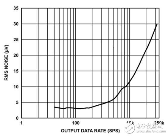
Figure 2. Relationship between rms output noise and output data rate
The effective resolution is expressed in number of bits, and the formula for converting to the 20 V full-scale input range is:
Effective resolution = log2 (FSR / rms noise)
Effective resolution = log2 (20 V/30 μV) = 19.3 bits
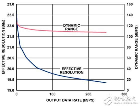
Figure 3. Effective resolution (root mean squares) versus output data rate
First, the rms noise is converted to an approximation of the peak-to-peak noise (root mean square noise multiplied by a factor of 6.6), and the effective resolution can be converted to noise-free code resolution. The result is approximately 2.7 bits, which is then subtracted from the effective resolution to obtain a noise-free code resolution. As shown in this example, after calculation, the 19.3-bit effective resolution is equivalent to 16.6-bit noise-free code resolution. This result is approximately 0.3 bit different from the 17.7-bit noise-free bit specification of the AD7176-2 with an unbuffered short-circuit input and an output data rate of 250 kSPS. This is because this example uses only ±10 V as the full-scale range, not the maximum value of ±12.5 V.
Figure 4 shows the system integral nonlinearity obtained using the endpoint method, expressed in ppm of full scale (FSR).
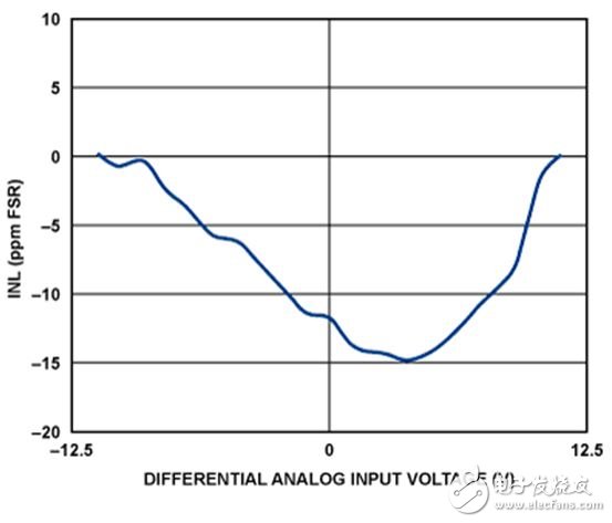
Figure 4. Integral nonlinearity (INL, expressed in ppm of FSR) versus input voltage
Although this circuit is primarily designed to handle DC input, it can also convert low frequency AC inputs. The distortion performance varies with the amplitude of the analog input. Figures 5 and 6 show the performance of -1 dBFS and -6 dBFS and 1 kHz sine wave, respectively. The sine wave generated by the Audio Precision 2700 series audio source is directly input to the AD8475.
Figure 5. FFT performance of the AD8475 to AD7176-2 (1 kHz, -1 dBFS input tone, 16384 point FFT)
Figure 6. FFT performance of the AD8475 to AD7176-2 (1 kHz, -6 dBFS input tone, 16384 point FFT)
For the best high-resolution system performance, excellent printed circuit board (PCB) layout, grounding, and decoupling techniques are essential. For details, please refer to the guide MT-031, Guide MT-101, AD8475 data sheet and AD7176-2 data sheet. For a complete schematic and printed circuit board layout, see the CN-0310 Design Support Package.
Traffic Safety Sign,Prohibition Traffic Sign,Led Traffic Sign Board,Led Traffic Sign Light
Jiangsu Bosiwei Optoelectronics Group Co.,ltd , https://www.bswledled.com