Foreword
In recent years, white light LEDs have the advantages that traditional light sources can't match in terms of luminous efficiency, power consumption, longevity and environmental protection, making white LEDs gradually replace incandescent bulbs and fluorescent lamps, and various governments have announced and proposed to disable incandescent bulbs. The timetable has accelerated this trend even more.
The mechanism for the generation of white LEDs can be divided into the following types: (a) The conversion of the blue light-emitting chip plus the Nd-YAG phosphor to the white LED is proposed by Nichia Chemical Co., Ltd. [1, 2] . (b) Conversion to a white LED with a violet light chip and an RGB color phosphor is still in the experimental stage. [3-5] (c) Blending white LEDs [6, 7] using RGB. At present, most of the products on the market are mainly converted into white LEDs by the Blu-ray chip and Nd-YAG phosphors. Therefore, how to improve the luminous efficiency of the Blu-ray chip is crucial for the development of white LEDs.
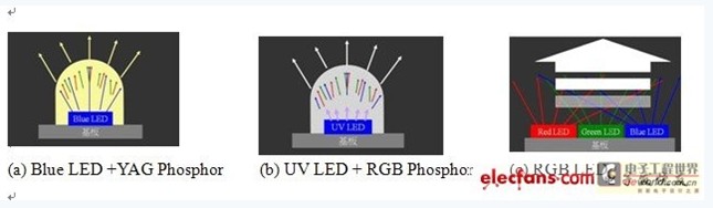
Figure 1 Mechanism of white LED generation (a) Blue LED+YAG Phosphor(b)UV LED+RGB Phosphor(c)RGB LED
The luminous efficiency of a semiconductor LED depends on the characteristics of the material itself. When the LED is injected with an extra carrier, the composite of the additional carrier is divided into a radiation composite (the additional carrier of the band can be combined to emit light) and the non-radiative composite (phonon composite release). The combination of heat and Oujie), in addition to the defect level between the bands, also captures additional carriers and reduces the chance of additional carrier recombination. Therefore, in recent years, many research teams have studied the illuminating mechanism by analyzing the fluorescence measurement technology in order to study how to improve the luminous efficiency of LEDs.
Fluorescent illumination mechanism
Fluorescence is a phenomenon in which electromagnetic radiation is emitted. For any material, when the incident photon energy is equal to or exceeds the energy band, the valence band electrons are excited across the energy band to reach the conduction band. When the excited state electrons return to the valence band from the conduction band, radiation is generated. Radiation, the production process is mainly divided into two stages as shown in Figure 2. (a) For excitation, additional carrier generation and excitation (b) is energy release and recombination, and the energy of the extra carrier in the excited state is released and combined (c) is a fluorescent photon signal generated by fluorescence generation.
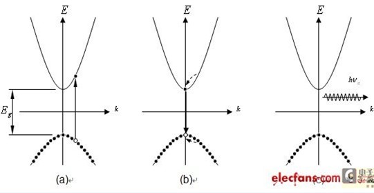
Figure 2 Fluorescence generation process
The way in which the fluorescence is generated is roughly divided into two types, namely, irradiating the sample with photons higher than or equal to the energy of the energy gap to generate additional carriers, or increasing the carrier concentration by electron injection to increase the probability of fluorescent photon generation. In order to increase the intensity of the fluorescent signal. These two types of methods are called photoluminescence (PL) and electro-excitation fluorescence, respectively. The illumination of LEDs is electrically excited, but the measurement of electro-active fluorescence must be embedded in the electrodes. It is indicated that photoexcitation fluorescence must be used in the process prior to embedding the electrode.
Since the laser can be used to provide sufficient power to excite the signal [8], the incident light begins to use the laser source. When the excited state electrons return to the ground state, a photon is generated, and many phonons are generated. It is assumed that the light source used is a continuous wave, and the fluorescent light excited thereby can be regarded as a steady state, and the test piece is continuously irradiated with fluorescence by the light source [9], and the fluorescence spectrum of the laser spectrum and the excitation is shown in Fig. 3.
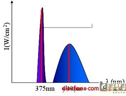
Figure 3: Fluorescence spectrum of laser and excitation
As can be seen from the Jablonski energy diagram [10] proposed by Alexander Jablonski in Fig. 4, the absorption of incident light is related to the wavelength of the incident photon, that is, the absorption of the material is related to the wavelength of the incident light source.
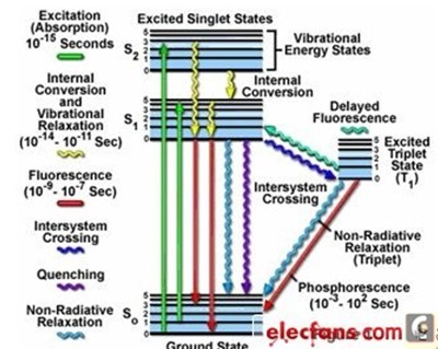
Figure 4 Jablonski energy diagram [10]
When the sample absorbs the incident light, it excites the electron to a higher energy state. After a period of time, the electron will release energy to a lower energy state. Impurities and defects form various energy levels in the energy gap, and their corresponding energy will be generated by radiation, such as photoexcitation, or by non-radiative recombination process [8][11], such as Phonon emission, defect capture, or the Oujie effect [12].
In addition to the above-mentioned conduction band and the valence band and Other energy band conversion will emit fluorescence, the defect will also cause the generation of fluorescence, as shown in Figure 5. Among them, EC, EV and ED are conductive strip, valence band and defect band respectively, wherein the defect band is distributed between EC and EV, the position and quantity depend on the material quality, and (a) is the band in Fig. 5 The electron hole is composited, (b) and (c) are all composites of defects, (b) the electrons of the conduction band are captured by the defects between the energy bands, and (c) the electrons and the valence band for the defect capture. Composite, the emitted fluorescent band depends on the distance between the electron and the hole before the composite.
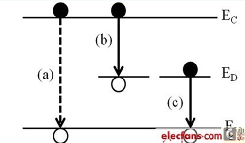
Figure 5 Radiation recombination (a) Electron hole-to-composite between the energy bands (b) Electron and valence band electro-combination if the defective electrons between the bands are trapped by the defect (c)
Light excitation fluorescence measurement
The main structure of PL spectrometer is excitation source, spectrometer, computer and cryogenic system. The architecture is shown in Figure 6.
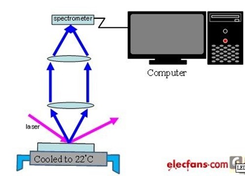
Figure 6 PL spectrometer architecture diagram
Since the blue LED band can be around 2.75 eV, the excitation source uses a wavelength of 325 nm (energy of 3.8 eV), 375 nm (energy of 3.3 eV) and 405 nm (energy of 3 eV) greater than its capable laser. The spectrometer scans between 350 nm and 700 nm. In addition, because the temperature has a great influence on the fluorescence intensity of the radiation composite, the measurement environment must be temperature controlled. Taking the blue LED as an example, the PL fluorescence spectrum is shown in Fig. 7. The excitation source is a 405 nm laser, the blue LED peak is at 461 nm, and the full width at half maximum is 25.2 nm.
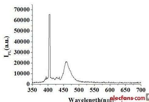
Figure 7 PL fluorescence spectrum
PL introduces the advantages of LED material analysis
Due to the fast measurement characteristics of PL, it can adapt to the production speed on the LED production line, and the non-contact and non-destructive measurement can ensure that the sample will not change the characteristics of the sample during the measurement process, with the mapping technology or The signal receiver is changed to CCD, the characteristics of the spatial distribution of the sample can be obtained, and the uniformity of the process can be known to feed back the MOCVD process. In the measurement, no electrode can be used to monitor the change of each step in the manufacturing process, which is the amount of PL. The advantages of measuring technology into the LED Wafer production line.
In the design and verification of LED components, indium gallium nitride, which is commonly used as a blue LED, is taken as an example. In the lattice constant and energy width diagram, the parabola connecting the two points of gallium nitride and indium nitride is nitriding. Indium gallium, as the indium content of indium gallium nitride increases, its energy level width becomes smaller [13,14], so the indium content of indium gallium nitride can be known from the position of the PL fluorescence spectrum peak. The laser intensity of the modulated excitation source and the spectral intensity of the measured fluorescence can be fitted to the correlation coefficient of the luminous efficiency of the LED, and then the internal luminous efficiency of the LED is obtained to provide verification of the component design, and no electrode is required for the measurement. At any step of the process, the process parameters can be changed, or different process methods can be selected to compare the PL fluorescence spectrum to optimize the optimal process conditions.
in conclusion
PL is a fast, non-contact, non-destructive measurement technique for the spatial distribution of measurable samples, and is well suited for both mass production and development of products.
"Lithium battery" refers to a battery made of lithium metal or lithium alloy as a negative electrode material, using a non-aqueous electrolyte solution.It has a high energy density.Compared with high-capacity nickel-cadmium batteries, the energy density is twice as high.High voltage. The average service voltage is 3.6v, which is three times higher than nickel-cadmium and nickel-hydride batteries.The use voltage is even and the high capacity, the widespread use temperature -20 degrees -60 degrees, the charge and discharge life is long, after 500 discharges its capacity at least has more than 70%.Due to the characteristics of high energy density, high voltage and stable operation, lithium battery is widely used.
Lithium Ion Battery Pack,12V Lithium Ion Battery Pack,12V Lithium Battery Pack,Lithium Battery Pack
Xinxiang Taihang Jiaxin Electric Tech Co., Ltd , https://www.agvchargers.com