Utilize the physical layer of the current 802.11b wireless network card and the EPXA1 development board of Altera Corporation to implement a software radio platform that can send and receive 802.11b wireless network signals. Based on this platform, various wireless LAN media access control protocols can be freely developed.
The development of wireless local area network access control (MAC) protocol is currently a hotspot in various wireless application research. At the same time, the development, debugging and implementation of the MAC protocol are inseparable from the support of the physical layer (PHY). Many developers of MAC protocols can only stay in the phase of protocol emulation because they do not have physical layer support. This paper proposes a wireless MAC development platform that can send and receive signals over a wireless link (which can communicate with 802.11b-based wireless LAN APs and wireless network cards). The platform utilizes the physical layer portion of the existing 802.11b wireless network card (including antenna, RF chip, IF chip and baseband processor), plus the EPXA1 development board. With this platform, various MAC protocols can be developed and debugged on the EPXA1 development board.
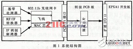
The system is mainly composed of three parts: 802.11b wireless network card, EPXA1 development board and the transfer PCB between the two, as shown in Figure 1.
The 802.11b wireless network card used in the system is connected to the notebook via a standard PCMCIA interface. The biggest feature of the wireless network card is that the MAC control chip and the baseband processing chip and the RF chip in the front end are separated, so that the MAC chip can be replaced with the EPXA1 development board. Before the wireless network card is started, the baseband processing chip and the control registers of the front-end IF and RF chips must be set to appropriate values. This is the work to be done in the control logic PLCI section. The main components of the network card are:
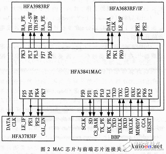
(a) HFA3841 (Wireless LAN Medium Access Controller) is the MAC part of the wireless network card. In this design, it is replaced with the author's development board.
(b) HFA3861B (Baseband processor) is the baseband processor of the wireless network card [3]. During the startup of the network card, it needs to be configured through the corresponding serial configuration port.
(c) The HFA3863A (RF/IF converter and synthesizer) chip performs RF to IF conversion [4], and the configuration register needs to be configured through the corresponding configuration port.
(d) The HFA3783 chip performs intermediate-to-baseband conversion [5], and the configuration of the registers (operating mode, operating frequency, etc.) is also required through the corresponding configuration port.
Altera's EPXA1 development board integrates the ARM922T embedded microprocessor and its corresponding peripherals. It has a programmable logic device with 100,000 equivalent system gates and corresponding expansion I/O ports in its peripherals. No additional FPGA circuit design is required. It is more convenient for the collaborative design of software and hardware. At the same time, Altera's QnartusII software also provides good support for hardware and software co-design.
The transfer PCB board is used to connect the extended I/O port of the EPXA1 development board with the useful signal lines on the 802.11b wireless network card. A PCMCIA slot is designed on the board to fix the wireless network card. The Adapter board uses the isolation chip SN74CBTD3384 for level conversion and protection of the EPXA1 development board, and also supplies power to the wireless network card through the board.
2 design process2.1 Handling of 802.11b wireless network cards
First, remove the MAC chip of the wireless network card, and then pull out the line connecting the baseband processor, the front-end radio, and the intermediate frequency chip on the MAC chip, because the front-end chip needs to be configured through these lines during the startup process of the network card. Figure 2 shows the connection between the MAC chip of the wireless network card and other chips. In the design process, it is necessary to ensure that these lines are led out to the EPXA1 development board.
2.2 Design of the transfer PCB board
Refer to the PCMCIA interface standard, connect the power and ground lines and the useful address and data lines to the extended I/O port of EPXA1 (logic high level is 5V). The connection process uses SN74CBTD3384 for level conversion ( 5V to 3.3V conversion). In addition, in the extended I/O port of EPXA1, there are pins that provide 3.3V and 5V power supply, which can be used as the power supply for wireless network cards. Test pins can also be added on the PCB to facilitate hardware debugging.

2.3 Design of PLCI part
The architecture of the entire system and the location of the PLCI are shown in Figure 3. PLCI (physical layer control interface) and PLDI (physical layer data interface) are the focus of the design. They are implemented using the programmable logic of EPXA1. The main programming language is Verilog HDL. PLCI is the control interface between the MAC and the physical layer. It implements the configuration of the control registers for the front-end chips (including the HFA3861B, HFA3683, and HFA3783), including the serial data, clock, and chip select signals required to generate the configuration. PLDI is the data interface between MAC and physical layer, which is the path for MAC and PHY to exchange data. ARM9 embedded microprocessor runs C language code to implement various wireless MAC protocols. The ARM9 is connected to peripheral devices via the AHB bus.
Before writing a program, first understand the read and write process of each control register.
The control interface of BBP (baseband processor) is a typical three-wire interface, that is, only three signals of clock (SCLK,) data (SD) and chip select (CS_BAR), there is no separate read/write enable signal, and it faces early use. The highest bit of the address is used to identify the read or write operation. Each time a read/write operation occurs, the serial address and data appear successively on the data line (SD), wherein the MSB (A7) of the address bit is a write operation, indicating that data is written into the register corresponding to the address; When the address bit MSB (A7) = 0, it is a read operation, and the data following the surface is read from the register indicated by the address.
HFA3683 and HFA3783 read and write timing is the same, through LE_RF and LE_I effective (low effective) to determine which chip to read and write.
The serial data on the DATA line is written to a 20-bit shift register in the chip on the rising edge of the clock, and then the address corresponding to the two bits of LSB1 and LSB2 is written on the rising edge of LE.
The serial output data (SD) and clock (SCLK) described above are generated by PLCI logic. Each front-end chip uses the rising edge of the clock to collect data, so the data is strictly aligned with the rising edge of the clock, with sufficient settling time and hold time.
In the design of PLCI, some registers are defined to communicate with the CPU. These registers have different widths according to the requirements of the corresponding chip read and write timing. For example, the write register of BBP has 17 bits, and the lower 8 bits are the data to be written. The 8 bits are the address of the register to be written, and the most significant bit is used to indicate whether the write operation is completed. In order to start the next read and write operation.
ESS (Excalibur Strpe Simulator) is a Stripe simulation model that simulates the execution of CPU instructions and is used to observe the bus timing of PLD to Stripe and Stripe to PLD. The AXD debugger with ADS 1.2 can be used by the module CPU to execute instructions and observe the state of the system after each instruction is executed.
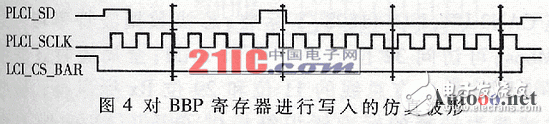
Through the combination of AXD Debugger and ESS, you can observe the timing of the corresponding bus on the PLD-to-Stripe or Stripe-to-PLD bus operation instruction, and then simulate it with ModelSim, which is convenient for debugging the program. Figure 4 is a simulation waveform of the BBP configuration in ModelSim, which is consistent with the write logic of the required BBP.
3 system startup and verificationBefore starting the system, you must also write a PLCI.C file, in which the c function is used to read and write the registers defined in PLCI.V.
//BBP write operation function
Void BBP_wr(long val)
{
*BBP_WRITE=vall0x8000;
//The upper eight bits of val are the address, the lower eight bits are the data, and the highest bit is the write register operation.
While(((*BBP_WRITE)&0x10000)==0x10000){}
/ / Read the flag bit, until the operation is completed
}
The write operation functions of the RF and IF chips are similar.
The BBP has a total of 49 registers to be written.
The HFA3683 has three control registers to write to, and the HFA3783 has four control registers. The registers common to the latter two chips are: mode register M (used to control the operating mode of the chip), R counter register and A/B counter (used to control the integrated frequency of the frequency synthesizer), R counter and A/B counter The specific value needs to be measured for the radio frequency and intermediate frequency of the wireless network card when working. According to one of the provisions of the 802.11b protocol, the wireless network card works with 14 channels [2], so the obtained RF chip (HFA3683A) has 14 operating frequencies (that is, 14 different R, A, and B values), and the intermediate frequency. (HFA783) The chip has one operating frequency.
The programming tool used is the Quartus II software, which can compile the hardware part (PLCI.V mainly or verilog HDL language) and the software part (PLCI.C) separately, and then compile and generate the .hex file to download to the development board.
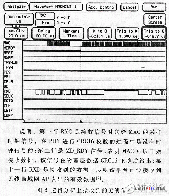
Verification process: Set the wireless network card to the receiving state (RX_PE is set high, TX_PEL is set low, RADIO_PE is set low, PE1 is set high, PE2 is set high, RESET is set high, and TR/SW is set low). In addition, you need to set up an 802.11b AP (Access Point), set it on a fixed working channel, and set the RF/IF Converter control register so that the network card also works on the channel. At this point, the logic analyzer is used to monitor the three signals from the BBP: RXC, RXD, MD_RDY signals, and the waveform shown in Figure 5 can be obtained in the logic analysis.
The system provides a serial data link to the MAC with a maximum rate of 22 Mbps. Combined with the embedded microprocessor on the EPAX1 development board, various WLAN demonstration systems can be built. Using the existing wireless network card as a physical layer can provide more convenience to those who focus on the development of upper layer protocols. As long as there is corresponding control logic, this system construction method is also applicable to other development boards, which brings a shortcut to those who want to verify and implement their own MAC protocol. I am currently using this platform to develop the 802.11e media access control protocol.
Hdmi Cables,Hdmi Cord,Micro Hdmi Cable,Extra Long Hdmi Cable
UCOAX , https://www.jsucoax.com