Nowadays, cardiovascular diseases have become one of the most important diseases that threaten human health. Clear and effective electrocardiogram provides a basis for diagnosing such diseases. ECG acquisition circuit is a key part of ECG, and ECG signals are weak. The signal has a frequency range of 0.03~100 Hz and an amplitude of 0~5 mV. At the same time, the ECG signal is also doped with a large number of interference signals. Therefore, a well-designed filter circuit and a suitable controller are obtained. The key to effective ECG signals. Based on this, this paper designs an ECG acquisition instrument with STM32 as the control core and AD620 and OP07 as the analog front end. The design is simple and practical, and the noise interference is effectively suppressed.
1 overall design
ECG acquisition includes two parts: analog acquisition and digital processing. This design collects ECG signals from the AgCl electrode and the three-lead ECG acquisition line, through the preamplifier circuit, bandpass filter circuit, 50 Hz double T notch The amplitude of the ECG signal is controlled by the main amplifier circuit and the level up circuit in the A/D acquisition range of the STM32. The STM32 sets the A/D sampling frequency through the timer, and performs the mean digital filtering on the obtained digital signal. Processing, and finally depicting the ECG graphics on the color screen, the overall block diagram of the system is shown in Figure 1.
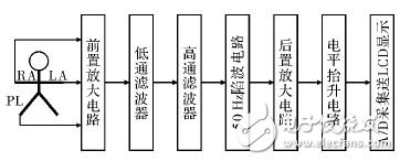
Figure 1 overall system block diagram
2 hardware design
2.1 main control module circuit design
The STM32F103VET MCU of the main control module is the core of the controller. The MCU is a 32-bit high-performance, low-cost and low-power enhanced MCU produced by ST STMicroelectronics. Its core adopts the latest Cortex-M3 architecture produced by ARM. The maximum operating frequency is 72 MHz, 512 kB of program memory space, 64 kB of RAM, 8 timers/counters, two watchdogs and one real-time clock RTC. The on-chip integrated communication interface has two I2Cs and three SPIs. Five USARTs, one USB, one CAN, one SDIO, and integrated with 3 ADCs and one DAc with 100 I/O ports. The main control chip pin arrangement diagram is shown as in Fig. 2.
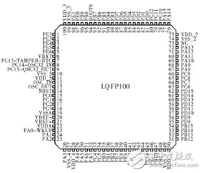
Figure 2 STM32F103VET microcontroller pin arrangement diagram
2.2 Design of preamplifier circuit
The preamplifier circuit is the front end of the analog signal acquisition, and is also the key to the whole circuit design. It not only requires accurate acquisition of the weak ECG signal from the human body, but also minimizes the interference signal. Since the ECG signal belongs to the differential signal, Therefore, the circuit should adopt a differential amplification structure, and the system is required to have high common mode rejection ratio, high input impedance, low drift and the like. Therefore, it is very important to choose the right op amp. Here, the instrument is preamplifier with the AD620 op amp. The AD620 features high precision, low noise, low input bias current and low power consumption, making it suitable for medical applications such as ECG monitors. application. The amplification factor of the AD620 is determined by the feedback resistance between the 1 and 8 feet. The gain G=49.4 kΩRG+1. Since the ECG signal contains a large DC component, the amplification factor of the preamplifier circuit cannot be too large. The selection is about 10 times, so the feedback resistor R6 takes about 5 kΩ. In order to improve the common mode rejection of the circuit, an OP07 is used to detect R10, and the common mode signal on R4 drives the wire shield to eliminate the distributed capacitance. At the same time, another OP07 op amp and R5, C3, and R7 form the right leg drive circuit. The common mode signal detected on R10 and R4 is passed through the inverting amplifier and then fed back to the human right leg via R7, further suppressing the common mode. Signal and 50 Hz power frequency interference, where the right leg drive has a feedback path to the alternating current, and the interference of the alternating current may cause harm to the human body. Therefore, attention should be paid to the insulation measures here, and the protection resistor R7 is as large as possible, taking 1 MΩ or more. . In addition, the instability of the system power supply also has a great impact on the acquisition of ECG signals. Therefore, in this system, the power supply pins of all op amps are decoupled with two 0.1μF and 10μF capacitors in parallel to improve the stability of the system. The circuit diagram of the amplifier circuit is shown in Figure 3.
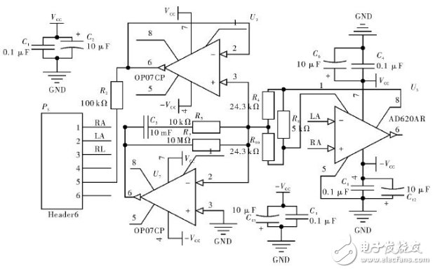
Figure 3 preamplifier circuit
2.3 Bandpass filter design
The ECG signal output from the preamplifier circuit also contains large DC components and EMG signals, and the interference components such as baseline drift. The useful ECG signals to be collected are in the range of 0.03~100 Hz, so it is necessary to design a reasonable filtering. The signal in this range is fully passed, and the signal outside the range is maximally attenuated. Here, two OP07 op amps with high precision, low offset and low power consumption are respectively composed of second-order active high-pass. Filter and low-pass filter, high-pass filter consists of C11, C17, R7, R10, cutoff frequency f1 ≈ 0.03 Hz, low-pass filter consists of R8, R9, C10, C13, cutoff frequency is about f2 ≈ 100 Hz The circuit of the system bandpass filter is shown in Figure 4.
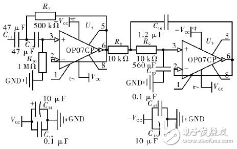
Figure 4 Bandpass filter
2.4 50 Hz double T notch design
Power frequency is the most important and most common source of interference in ECG signals. Although the front right leg drive circuit has a certain inhibitory effect on it, a large part of it enters the latter circuit. Therefore, it is necessary to design the cutoff frequency as A 50 Hz band-stop circuit is used to further filter out the interference. The band-stop circuit is also called a notch filter. As the name implies, the band-stop circuit is to greatly attenuate the signal in a certain frequency range, and has little effect on the signal outside the frequency range. . The double T trap circuit is a typical band stop circuit. In the dual T network, the parameters of the two T-type networks are symmetrical. In the 50 Hz double T trap circuit shown in Figure 5, R13=R14=2R16= R=32 kΩ, C20=2C19=2C18=C=200 nF, essentially consisting of two T-type high-pass filters and a low-pass filter in parallel. The cut-off frequency of the circuit shown in Figure 5 is f0=1/2πRC≈50 Hz.
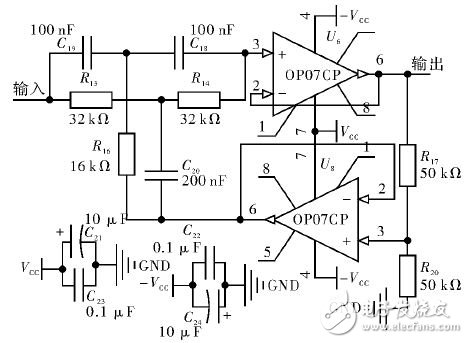
Figure 5 50Hz band stop filter
2.5 main amplification and level up circuit design
The amplitude of the ECG signal is about 0~4 mV, and the input level of the STM32 AD conversion is 3.3 V. Therefore, in order to process the acquired ECG signal, the acquired analog signal needs to be amplified by 800~1 000 times. The preamplifier circuit has been amplified by 10 times. In theory, the main amplifier circuit can be amplified by about 100 times. In order to ensure that the signal is not distorted, the single-stage amplification is generally no more than 10 times. Therefore, the two-stage amplification method can be used to achieve the effect of enlarging 100 times, the U9 fixed amplification is 10 times, and the U11 feedback resistor is an adjustable resistor, so that The effect of amplifying 100 is achieved by the adjustment of the varistor. In addition, because the A/D acquisition of STM32 MCU can not collect negative level, the level raising circuit as shown in U7 is designed to mention the ECG signal above 0 level, which is convenient for MCU acquisition.
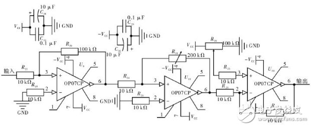
Figure 6 main amplification and level up circuit
3 software design
After getting the ECG signal, input STM32 for AD acquisition and software filtering, and finally send the LCD to realize the waveform display. After the microcontroller is initialized, the programming timer is interrupted every 6 ms. In the interrupt function, the read A/D value is read. The mean filtering is used to filter out the interference, and then the coordinate value corresponding to the color screen is converted, and the waveform is displayed on the color screen to realize the real-time display of the waveform. The program flow of the whole system is shown in FIG. 7 .
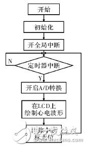
Figure 7 system software flow chart
4 test results analysis
The electrocardiographic signals obtained by the front-end analog circuit and the STM32 are processed by the front-end analog circuit and the STM32 in the left arm, the right arm, and the right leg of the person through the electrode pad and the three-lead wire, and finally the ECG signals obtained on the oscilloscope and the color screen are as shown in FIG. 8 .
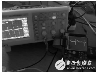
Figure 8 system effect display
From the ECG obtained from the color screen and the oscilloscope, the 50 Hz power frequency signal and the baseline drift are better suppressed. As can be seen from the oscilloscope, the time between the adjacent two peaks is about 900 ms, which is true. The ECG signal is basically consistent, the image is clear and stable, and it can better reflect the ECG characteristics of the human body.
5 Conclusion
This design realizes a small ECG collector with STM32 as the control core and AD620 and OP07 as the analog signal acquisition terminal. The ECG waveform measured by this design is basically normal, the noise interference is effectively suppressed, the circuit performance is stable, and the home monitoring is basically satisfied. As well as the requirements of pathological analysis, the whole system is simple in design, low in cost, and has certain medical value.
It can be equipped with different type of storage battery such as lead acid battery, Nickel Cadmium Battery, silver zinc battery, Lithium Ion Battery and other storage batteries, providing various output voltage classes.
Built-in storage battery and charger, equipped with the function of over-charge and over-discharge protection and capacity display. It is used as working power supply for lightings, communications, laptops, and special instruments of emergency working, field working, press interviews, special vehicles and other fields.
Dc Power Supply,110V Dc Power Supply,220V Dc Power Supply,110V Dc Power Supply System
Xinxiang Taihang Jiaxin Electric Tech Co., Ltd , https://www.chargers.be