Abstract: The basic principle and manufacturing method of low-cost square wave inverter Power Supply are proposed. The use of drive circuit chip SG3524 and IR2110 is introduced. The drive and protection circuit are designed. The experimental results of output voltage waveform are given.
This article refers to the address: http://
Keywords: inverter; bootstrap capacitor; low cost
0 Preface
The power supply is the power part of the electronic device and is a highly versatile electronic product. It has been widely used in various industries and daily life. Its quality greatly affects the reliability of electronic equipment. Its conversion efficiency and load-bearing capacity are directly related to its application range. Square wave inverter is a low-cost, extremely simple conversion method. It is suitable for various rectification loads, but it is not very suitable for the load of the transformer and has a large noise.
Based on the basic principle of inverter power supply, this paper proposes a method for making and debugging a square wave inverter by using the analysis and derivation of existing data.
1 System basic principles
The input end of the inverter power supply is a battery (+12V, capacity 90A·h), and the output end is a power frequency square wave voltage (50Hz, 310V). Its structural block diagram is shown in Figure 1.
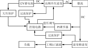
Figure 1 Block diagram of the square wave inverter
At present, there are many new technologies constituting DC/AC inverters, but considering the specific use conditions and cost and reliability, the power supply still uses typical secondary conversion, namely DC/DC conversion and DC/AC inverter. Firstly, the DC 12V voltage is inverted into a high-frequency square wave by DC/DC conversion, boosted by a high-frequency step-up transformer, and then rectified and filtered to obtain a stable DC voltage of about 320V; then converted by DC/AC to square wave inverter. The method converts the stable DC voltage into a square wave voltage with an effective value slightly larger than 220V; and then obtains a 50Hz AC voltage with an effective value of 220V through LC power frequency filtering to drive the load.
2 DC/DC conversion
Since the primary side voltage of the transformer is relatively low, in order to improve the utilization rate of the transformer and reduce the cost, the DC/DC conversion is as shown in Fig. 2. The push-pull circuit is used, the primary side center tap is connected to the battery, and the two ends are controlled by the switch tube, and alternately work. Can improve conversion efficiency. The push-pull circuit uses fewer switching devices, and the double-ended transformer has a smaller volume, which can increase the duty ratio and increase the output power.
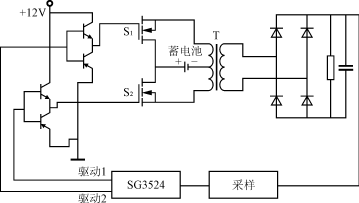
Figure 2 DC / DC conversion structure
The square area product of the square-wave inverter transformer with double-ended operation is
A e A c = P o (1+ η )/( ηDKjfK e K c B m )(1)
Where: A e (m 2 ) is the cross-sectional area of ​​the core;
A c (m 2 ) is the window area of ​​the core;
P o is the output power of the transformer;
η is the conversion efficiency;
δ is the duty ratio;
K is the waveform coefficient;
j (A/m 2 ) is the average current density of the wire;
f is the inverter frequency;
K e is the effective coefficient of the core section;
K c is the window utilization factor of the core;
B m is the maximum magnetic flux.
The switching tubes S 1 and S 2 of the primary side of the transformer are only connected in parallel by IRF32055. The reason why they are connected in parallel is mainly because the current of the primary side of the transformer is relatively large when the inverter is connected to the load, and the parallel connection can be divided, which can effectively reduce The power consumption of the switch tube will not cause damage.
The PWM control circuit chip SG3524 is a voltage type switching power supply integrated controller with output current limiting, adjustable switching frequency, error amplification, pulse width modulation comparator and shutdown circuit, which generates peripheral lines required for PWM square wave. Very simple. When the foot 11 is used in parallel with the foot 14, the duty cycle of the output pulse is 0 to 95%, and the pulse frequency is equal to 1/2 of the oscillator frequency. When the foot 10 (off terminal) is added with a high level, the output pulse can be blocked, and the external circuit can be properly connected to realize the undervoltage and overcurrent protection functions. Use the SG3524's internal operational amplifier to adjust the duty cycle D of the output drive waveform so that D >50%, then after the CD4011 is reversed, D <50% of the drive waveform of the tube is obtained, thus ensuring two groups. When the switch is driven, there is a common dead time.
3 DC/AC conversion
As shown in Fig. 3, the DC/AC conversion adopts single-phase output and full-bridge inverter form. In order to reduce the volume of the inverter power supply and reduce the cost, the output uses power frequency LC filtering. The bridge inverter circuit is composed of 4 IRF740s. The IRF740 has a maximum withstand voltage of 400V, a current of 10A, and a power consumption of 125W. The drive signal is provided by the half-bridge driver IR2110. The input waveform is provided by the SG3524. Similarly, the output drive waveform of the SG3524 can be adjusted. The D <50% guarantees that the inverter's driving square wave has a common dead time.

Figure 3 DC / AC inverter circuit structure
The IR2110 is a high-power MOSFET and IGBT-specific driver IC manufactured by IR. It can achieve optimal driving of MOSFETs and IGBTs. It also has fast and complete protection functions, which can improve the reliability of the control system and reduce the complexity of the circuit. degree.
The internal structure and working principle of the IR2110 are shown in Figure 4. In the figure, HIN and LIN are the driving pulse signal input ends of the upper and lower power MOS of the same bridge arm in the inverter bridge. SD is the protection signal input terminal. When the pin is connected to the high level, the output signal of IR2110 is completely blocked, and its corresponding output terminal is always low. When the pin is connected to low level, the output signal of IR2110 follows HIN and The change in LIN, in the actual circuit, terminates the output of the user's protection circuit. HO and LO are the two drive signal outputs that drive the MOSFETs of the same bridge arm.
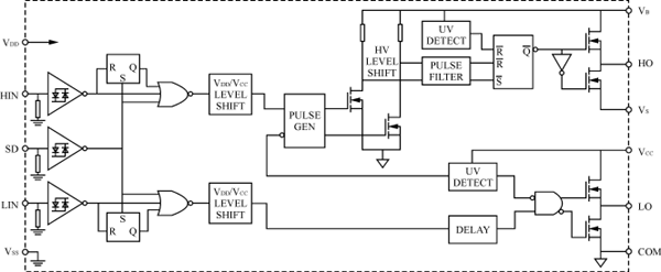
Figure 4 IR2110 internal structure and working principle block diagram
The bootstrap capacitor of IR2110 is not well selected, which may cause chip damage or malfunction. The capacitance between V B and V S is the bootstrap capacitor. The bootstrap capacitor voltage can reach 8.3V or above before it can work normally, or use a small capacitor to increase the charging voltage, or provide 10~20V isolated power directly between V B and V S. This circuit uses 1μF self. Lift the capacitor.
In order to reduce the output harmonics, the DC/AC part of the inverter generally adopts bipolar modulation, that is, the pair of tubes of the inverter bridge are high frequency complementary turn-on and turn-off.
4 Some problems in the design and debugging process of the protection circuit
The protection circuit is divided into undervoltage protection and overcurrent protection.
The undervoltage protection circuit is shown in Figure 5. It monitors the voltage condition of the battery. If the battery voltage is lower than the preset 10.8V, the protection circuit starts to work, so that the pin 10 of the controller SG3524 outputs a high level and stops driving. Signal output.
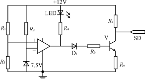
Figure 5 undervoltage protection circuit diagram
In Figure 5, the voltage at the forward input of the op amp is divided by R 1 and R 3 , and the voltage at the inverting input is clamped at +7.5 V by the Zener. When the voltage of the battery drops below a predetermined value, the operational amplifier Start work, the output jump is negative, the LED light is on, and the three-stage tube V is cut off, outputting a high level to the SD end of the SG3524, blocking the output drive signal of the IR2110.
The overcurrent protection circuit is shown in Figure 6. It monitors the output current condition and is preset to 1.5A. The output current of the square wave inverter is sampled into the inverting input terminal of the operational amplifier. When the output current is greater than 1.5A, the output of the operational amplifier jumps to negative. After the RS trigger composed of CD4011, the three-stage tube is made. The signal of the V 1 base level is low level, the three-stage tube is cut off, and the high level is output to the SD1 end of the IR2011 for protection purposes.
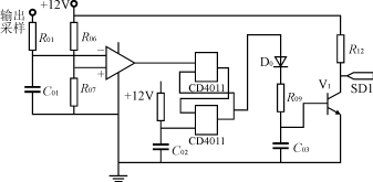
Figure 6 Overcurrent protection circuit diagram
A more important issue encountered during the debugging process is the selection of the bootstrap capacitor for the IR2110. The upper tube driver of the IR2110 is powered by an external bootstrap capacitor, which greatly reduces the number of driving power supplies, but also has certain requirements for the selection of the bootstrap capacitor between V B and V C . After the test, the 1μF electrolytic capacitor is finally used, which can effectively meet the requirements of the bootstrap voltage.
5 test results and output waveform
The output voltage of the DC/DC converter is stable at 320V, and the switching frequency of the IR2110 of the half-bridge driver of the control switch is 50Hz. The circuit waveform of the experiment is shown in Figure 7~14.
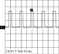
Figure 7 IR2110 lower tube driving waveform
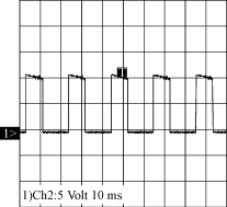
Figure 8 IR2110 upper tube drive waveform
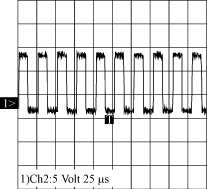
Figure 9 SG3524 output drive waveform (DC / AC)
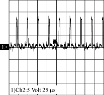
Figure 10 SG3524 drive waveform (DC / DC)
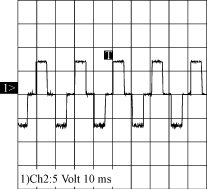
Figure 11 Output voltage waveform of external rectified load
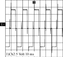
Figure 12 Output voltage waveform of an external 300Ω resistive load

Figure 13 Output voltage waveform of an external 500Ω resistive load

Figure 14 Output voltage waveform of an external 600Ω resistive load
6 Conclusion
Lightweight, small, and efficient in the development direction of inverter power supply is its goal. The inverter power supply circuit introduced in this paper mainly adopts integrated chip, which makes the circuit structure simple, stable performance and low cost. Therefore, this circuit is a circuit with simple control, high reliability and good performance. The entire inverter power supply is therefore highly cost-effective and competitive in the market.
Waterproof Power Supply,Waterproof Led Power Supply,Power Supply,Waterproof 12V Power Supply
Ninghai Yingjiao Electrical Co., Ltd. , http://www.yingjiaoadapter.com