This paper mainly focuses on the shortcomings of the existing LED driver circuit to shorten its life due to the existence of electrolytic capacitors. A design scheme of an LED driver circuit with no electrolytic capacitor is proposed. The scheme is based on the principle of extending the life of the circuit, based on the combination of switching power supply and linear power supply, making full use of its advantages, because the switching power supply has the characteristics of high efficiency energy conversion and the linear power supply has the characteristics of no output ripple. The design scheme fully utilizes its respective advantages to replace the electrolytic capacitor filtering, and effectively solves the problem that the existing LED driving circuit has a short life. This LED driver circuit has no large-capacity electrolytic capacitors. The small capacitors can use long-life capacitive components such as thin film capacitors, which make them have long life, high efficiency, low ripple current, and high safety and stability. .
1 Introduction
LED (Light Emitting Diode) is a new generation of green lighting source, which has many advantages such as energy saving, environmental protection, high brightness and long life. It is not only the new darling of lighting sources, but also related to people's lives. Therefore, the development of long-life driving power supply, the construction of high efficiency, low cost, high power factor and the key to LED lighting quality and overall performance, is also the need for the development of LED lighting technology. According to incomplete statistics, the life of existing incandescent bulbs is about 40 times less than that of LED lamps. Because the light-emitting diode is not only a DC current driving device but also a photoelectric converter, it has a function of converting photoelectricity. Its main function is to convert electric energy into light energy by flowing current, so its advantage is higher than the energy efficiency and working life of the general light source. However, it is generally required to use a large-capacity electrolytic capacitor in the rectifier circuit and the filter circuit of the LED driving power source. The life of an electrolytic capacitor is generally l05 ° C / 2000 h, which means that when the temperature around the capacitor rises to 105 ° C, its life is only 84 days, even in the environment of 85 ° C, the service life is only 332 days, so the electrolysis Capacitance is the main reason that hinders the life of LED driver circuits. In order to improve the life of the driving power supply, it is necessary to remove the electrolytic capacitor. For this reason, a high-brightness LED driving power source without an electrolytic capacitor is proposed.
2. LED driving circuit works
The overall block diagram of the circuit of this design is shown in Figure 1:
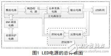
The circuit topology uses a flyback topology circuit that uses PWM to control the switching frequency to output a constant current and voltage to drive the LEDs. It mainly includes: pre-stage protection circuit, EMI filter circuit, rectifier circuit, RCD clamp circuit, synchronous rectification circuit, power conversion circuit, output filter circuit, feedback circuit, control circuit, etc.
In order to make the circuit less susceptible to electromagnetic interference, the EMI filter circuit is connected to the pre-stage protection circuit, which filters out the higher harmonics in the circuit and the surge in the circuit.
The input rectification section is composed of a bridge rectifier circuit and a π-type filter circuit respectively. Because the diode has a single-conducting characteristic, the bridge rectifier circuit can convert the alternating current into a unidirectional direct current, and then in the π-type filter circuit. Under the action, the output is stable DC voltage.
Then, the control circuit adjusts and controls the output to reach the design value. Finally, the output filter circuit reduces the output ripple to DC power, and finally outputs the DC power to the LED.
3. The specific design of the LED drive circuit
3.1 Input circuit design
The indicators of this design circuit are: input AC voltage Vin: 90-264 VAC/50-60Hz; output voltage Vo: 27VDC; output current Io: 0.68A.
As shown in Figure 2, the input circuit includes a safety device, an EMI noise filter, a bridge rectifier circuit, and a π-type filter circuit.
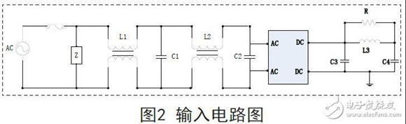
As shown in Figure 2, in order to reduce electromagnetic interference in the 1MHz band, the EMI noise filter circuit is composed of capacitors C1 and C2 and inductors L1 and L2. The safety device consists of a fuse and ZNR. When a spike current is generated, the fuse will quickly cut off the circuit to protect the load. ZNR is a surge absorber. When static electricity and surge occur at the input of the drive circuit, it will It becomes very impedance, so it can protect the circuit behind it. The bridge rectification filter circuit converts alternating current into direct current, and the subsequent π-type filter filters out voltage and current ripples in the circuit.
3.1.1 Design of EMI Filters
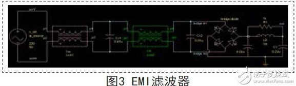
The EMI filter circuit diagram is shown in Figure 3. The EMI filter circuit is mainly used to attenuate differential mode interference by the differential mode capacitors CX1 and CX2 in front of the rectifier bridge.
In order to reduce the differential mode interference, a π-type differential mode filter composed of C1, C2 and L1 is added after the rectifier bridge. The differential mode capacitor in the EMI filter circuit uses X-amplifier capacitor, the safety level is X2, and its withstand voltage is 2500V, of which CX1=0.47uF, CX2=0.01uF. The common mode inductor LX1 is 7mH and LX2 is 1mH. After the rectifier bridge The C1 and C2 filter capacitors of the π-type filter circuit are selected from film capacitors with a withstand voltage of 450V, and their capacitance values ​​are 0.22uF; the differential mode inductor L1 is 1mH.
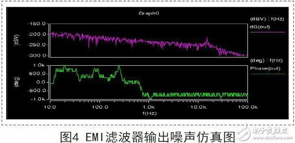
As can be seen from Figure 4, the noise signal will drop significantly when the frequency is higher than 1KHZ. It can be seen that the circuit can effectively reduce high frequency interference.