The advent of higher-order definition panel products is considered to be the best testimony to the enormous vitality of liquid crystal display technology. This view can not help but make people advance the advancement of liquid crystal technology with the emergence of OLED color TV and the elimination of LCD TV rival plasma TV.
This article refers to the address: http://
First of all, 4K technology is indeed a challenge for plasma. The biggest weakness of plasma display technology lies in the bottleneck of "pixel density." This is why plasma does not make 32-inch TVs. In fact, the 42-inch full HD resolution is already a very high pixel density for plasma technology. Once the market established a higher pixel density is a good product concept, plasma TV was forced to join this "PPI" as the standard of competition. This will be a very unfavorable phenomenon for plasma display technology.
Second, the most active panel companies that promote 4K color TV products are Sharp, AUO and Chi Mei. These three have a common feature, which is relatively insufficient in OLED technology reserves. As the world's No. 1 LCD sales company, the products on 4K are concentrated on more than 70 industrial and commercial products, and the 4K for the civilian color TV market, especially the 32-55 inch market, is conservative. LGD, the second largest global panel industry with similar strategy. On the other hand, Samsung and LGD are the first companies to promote OLEDs. This is reminiscent of some companies pushing 4K LCD to compete with the new hot OLED technology, or to delay the development of OLED.
There are people who hold the view that the 4K liquid crystal is placed on the opposite side of the OLED. Not only because of the difference between the two camps, but also because if the competition of high-end TV is based on 4K, OLED will inevitably have more technical difficulties in the initial mass production. However, this view ignores the fact that the premise of the large-scale emergence of 4K technology is the maturity of the new technology oxide TFT technology - this technology is precisely the technology necessary for the development of the OLED panel industry: he can not only be OLED The panel provides greater pixel density and helps with the life of the OLED panel.
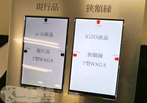
It is well known that OLEDs are current driven and LCDs are voltage driven. Compared with the conventional A-SI TFT and the metal oxide TFT, the biggest disadvantage is that the electron mobility is low, that is, the adaptability to the large current working condition is low. In addition, another technology widely used in medium and small size high pixel density liquid crystals, LTPS TFT can also greatly enhance the electron mobility and is widely used in OLED products of the same size. At present, LGD's 8.5-generation OLED will use metal oxide TFT, while Samsung's 8.5-generation OLED panel line is expected to adopt the traditional process at the beginning, and may evolve into Samsung's unique SGS (Super Grain Silicon) process LTPS TFT.
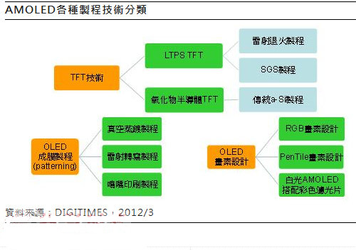
Therefore, in the case of most 4K or other high pixel density liquid crystals using LTPS TFT or metal oxide TFT technology, the technology upgrade and transfer of panel companies to the two is not only a negative competition for OLEDs, but a future. The production line was further upgraded to OLED and ready for the first step.
Secondly, the competitiveness of OLED technology in high pixel density products will not be worse than the current LCD: the most comprehensive Sharp of 4K LCD product line, and also the main promoter of high pixel density OLED. At the SID2012 show in 2012, Sharp showed a 13.5-inch organic EL panel with 3840×2160 pixels. This compares the latest 5-inch, 1920×1080 resolution LCD display panel from LG, and the pixel density is not much different. In addition, at SID2012, CMO exhibited TRIPOLED OLED panels with 3.4-inch and 4.3-inch resolutions up to 326ppi, and will be mass-produced in the fourth quarter of 2012. - The facts show that the PPI of OLED panels in the small size field does not lag behind any LCD products.
From a technical point of view, high pixel density LCDs and OLEDs use metal oxide or low temperature polysilicon TFT drive technology. At the same time, in the film-forming structure, OLEDs are not in the field of pixel density. On the contrary, OLEDs that exist in solid state once form a high-precision density structure, but are more stable than liquid LCDs. At present, the industrial bottleneck of the high pixel density film-forming structure of OLED materials mainly lies in: first, the preparation of large-scale glass substrate disposable film forming equipment, and second, and the development of low-cost film forming process equipment.
As far as the first point is concerned, Samsung's 5.5-generation line, code-named A2, is first cut into a quarter-5.5-line substrate and then an OLED film layer. However, another 5.5-generation line codenamed A3 that Samsung is building will use a non-cutting film-forming method. As far as the second point is concerned, the "evaporation film" technology currently used is indeed somewhat high for the large-scale large-scale preparation of OLEDs. However, Japanese and Korean companies have developed prototypes of OLED film-forming technology based on printing technology – a cost reduction of an order of magnitude.
From the development path of LCD high pixel density, we can see the rule that high pixel density products are gradually developed from small size to large size (small size close-range display products are more sensitive to pixel size). At present, small- and medium-sized OLEDs have completely broken through the process bottleneck of “high PPIâ€, which makes the view that “high pixel density LCD can prevent OLED popularization†almost bankrupt.
Guangzhou Winson Information Technology Co., Ltd. , https://www.barcodescanner-2d.com