Let's talk about the history of ARM: On December 5, 1978, physicist Hermann Hauser and engineer Chris Curry founded the Cambridge Processing Unit in Cambridge, England, to supply electronic equipment to the local market. In 1979, the CPU company was renamed Acorn Computer Corporation.
In the mid-1980s, a small team at Acorn chose the right processor for their next-generation computer. According to the technical requirements they provided, they could not find a suitable processor in the market at the time, so Acorn decided to design a processor. A small team completed the entire process from design to implementation in just 18 months. This is a computer with a RISC instruction set called Acorn RISC Machine (ARM). Later, Acorn was down, and the processor design department was separated to form a new company.
ARM mainly designs the ARM series AISC processor core. It does not produce chips and only provides IP cores. First explain the architecture, core, processor and chip with an example: S3C2440, this is a SoC chip, note that it is not cpu, 2440 and our well-known 51 MCU are similar, are embedded, embedded development Currently it has gone through three stages, namely SCM, MCU and SoC. 51 belongs to SCM or MCU, and 2440 belongs to SoC. Let's take a look at the internal structure of 51 single chip microcomputer.
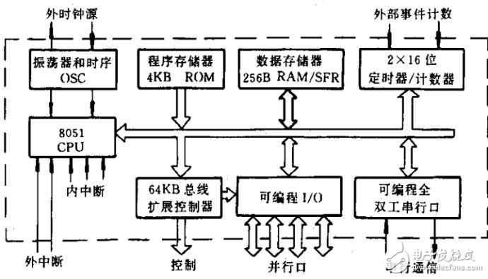
Its internal structure can be easily divided into two parts: cpu and peripherals. Look at the 2440:
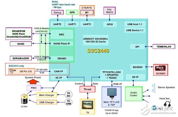
The arm920t in the middle is its processor. The processor and core are in my opinion here a concept, but one is a hard concept and the other is a soft concept. The 920t here is both a processor and a core. What Samsung does is something other than this cpu.
What about the architecture? Look at a picture again.
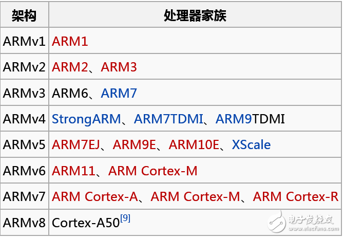
The left side is the architecture, the right side is the processor, or it can be called the core. Arm's first most successful cpu is ARM7TDMI, which is based on ARMv4. The ARM architecture includes the following RISC features:
Read/store architecture
Address misalignment memory access is not supported (ARMv6 kernel is now supported)
Orthogonal instruction set (arbitrary access instruction can access data in any addressing mode Orthogonal instrucTIon set)
A large number of 16 & TImes; 32-bit register array (register file)
The fixed 32-bit opcode length reduces the cost of coding and reduces the burden of decoding and pipelining.
Most are executed in one CPU cycle.
Different versions of the architecture will be adjusted.
The other major manufacturers that cooperate with ARM and Samsung usually put their CPUs and various peripheral IPs together, and then take the drawings to stream them. The squares produced are also a lot of pins. This thing not only contains the CPU, but also contains other controllers. This thing is called SOC (system on chip). From the perspective of English, the so-called quad-core SOC, the intention is not a single CPU, but a quad-core system.
So what the major manufacturers are doing now is to buy the ARM license, get the ARM processor source code, and then do some peripheral IP (or buy or design), form a SOC, go to the film. Different SOCs have different architectures (that is, how the CPU is connected with IP, some with the bus as the core, and some with the DDR as the core). Therefore, HiSilicon is the SOC architecture with independent property rights. However, no matter how any manufacturer, how to toss, there is no way to move the CPU, ARM core will stay there, that is the central processor.
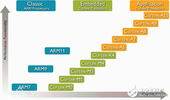
Currently ARM product ladder:
ARM naming rules:
The first number: series name: eg.ARM7, ARM9
The second number: Memory system
2: with MMU
4: with MPU
6: No MMU and MPU
Third number: Memory size
0: Standard Cache (4-128k)
2: Reduced Cache
6: Variable Cache
The fourth character: T: indicates support for the Thumb instruction set
D: indicates support for on-chip debugging (Debug)
M: indicates embedded hardware multiplier (MulTIplier)
I : Support for on-chip breakpoints and debug points
E: indicates support for enhanced DSP functions
J: indicates support for Jazelle technology, namely Java accelerator
S: indicates full synthesis
Lithium Battery Chargers,48V Lithium Battery Charger,48V Bike Lithium Battery Charger,48V Bicycle Lithium Battery Charger
Changxing Deli Technology Co., Ltd. , https://www.delipowers.com